
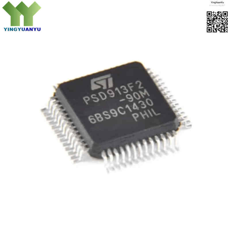
PSD913F2-90M
| Part Number | PSD913F2-90M |
|---|---|
| Manufacturer | STMicroelectronics |
| Category | Integrated Circuits (ICs) > Embedded – Microcontrollers – Application Specific (Programmable System Devices) |
| Description | High-performance 90ns Flash Programmable System Device (PSD) integrating 1Mbit primary Flash memory, a 256Kbit secondary Flash, 16Kbit SRAM, and highly flexible programmable logic gates for 8-bit microcontroller systems. |
| Stock Status | In Stock |
| Origin | Original Factory |
Product Overview
The PSD913F2-90M is ST’s integrated Programmable System Device (PSD) designed for 8-bit MCUs like 80C51, 68HC11 and Z80. It integrates dual independent Flash banks, 16K SRAM and programmable logic array on one chip, cutting PCB component count and layers. The 1M primary Flash stores firmware, while the 256K secondary Flash supports background IAP and secure boot. With 90ns fast memory access and PLCC-52 packaging, it is ideal for legacy telecom, grid meters and industrial control hardware.
Core Advantages
Dual-Bank Independent Flash Architecture
Integrates two independent Flash memory banks, allowing the system host MCU to read from one block while simultaneously erasing or writing data sectors into the other without disrupting code execution paths.
Integrated Programmable Logic Array (PLD)
Features an embedded programmable logic structure capable of decoding address paths, managing I/O extensions, and generating custom control signals, replacing discrete standard logic chips entirely.
In-System Programmability (ISP) via JTAG
Supports robust hardware configuration adjustments and firmware uploads directly onto the board via a standard built-in JTAG interface, streamlining production code flashing and post-assembly updates.
Advanced Built-In Power Management
Incorporates automatic power-down control circuitry that continuously monitors MCU bus activity, transitioning individual memory blocks into low-power states when idle to save system power.
Key Specifications
| Brand | STMicroelectronics |
|---|---|
| RoHS Status | RoHS Compliant options available |
| EDA/CAD Model | 3D Model & PCB Footprint Available upon request |
| Warranty | 1-Year Standard Factory Warranty |
| Package / Case | PLCC-52 Package |
| Mounting Type | Surface Mount / Socketable Installation (SMD/SMT) |
| Surface Marking / Silkscreen | PSD913F2-90M Marking |
| Primary Flash Memory Capacity | 1 Mbit (128K x 8 Architecture layout) |
| Secondary Flash Memory Capacity | 256 Kbit (32K x 8 Architecture layout) |
| SRAM Memory Capacity | 16 Kbit (2K x 8 Static Random Access Memory Matrix) |
| Memory Access Speed ($T_{ACC}$) | 90 ns Maximum Memory Cycle Propagation Delay Time |
| Programmable I/O Port Lines | Up to 27 Configurable Programmable I/O Pins Available |
| Microcontroller Interface Compatibility | Supports Multiplexed and Non-Multiplexed 8-Bit Address/Data Bus Structures |
| Operating Voltage ($V_{CC}$) | 4.5V to 5.5V High-Tolerance Operating Supply Range |
| Operating Temperature Range | 0°C to +70°C Commercial Temperature Grade |
Typical Applications
- Legacy Telecom Switching Interfaces, Network Routers, and Infrastructure Access Gateways
- Smart Industrial Utility Grid Meters, Digital Power Monitoring Panels, and Flow Controllers
- Industrial Process Automation PLCs, Distributed I/O Controller Blocks, and Motor Control Loops
- Point-of-Sale (POS) Terminals, Handheld Data Collectors, and Smart Ticket Dispensing Hardware
- Medical Monitoring Instruments, Laboratory Electronic Scales, and Environmental Sensor Interfaces
Order & Shipping Info
| Minimum Order Quantity (MOQ) | 1 Piece |
|---|---|
| Shipping Time | Shipped within 1-2 business days |
| Delivery Time | 3-7 working days worldwide |
| Shipping Methods | DHL, UPS, FedEx, EMS |
| Payment Methods | T/T (Bank Transfer), PayPal, Credit Card, Western Union |
Technical Support
For datasheet, sample requests, stock check, or bulk pricing, please use the Quick Inquiry form. We will reply within 24 hours.
Frequently Asked Questions
Q1: Is your currently available stock of the PSD913F2-90M component fully original and authentic?
A: Yes, we guarantee that all PSD913F2-90M programmable devices in our warehouse inventory are 100% brand-new, factory-original products from STMicroelectronics, stored and handled under strict ESD anti-static guidelines and moisture-controlled conditions.
Q2: What unique operational benefit does the independent secondary Flash memory bank provide?
A: The dual-bank layout allows the secondary Flash bank to securely hold bootloader codes or look-up tables. It enables true In-Application Programming (IAP), meaning the host MCU can execute code from the secondary block while updating or rewriting the main application program in the primary Flash bank.
Q3: How does the integrated Programmable Logic Device (PLD) help reduce total BOM cost?
A: The on-chip PLD handles custom chip-select logic, address decoding, and glue logic. This eliminates the need for separate discrete logic ICs (like 74-series logic chips), which reduces total component count, minimizes PCB routing traces, and lowers overall assembly cost.
Q4: How can our engineering development team download software configuration utilities, layout footprints, or request a volume discount quote?
A: Please complete our Quick Inquiry web form on this page with details about your processing parameters. Our application support desk will process your inquiry and dispatch the available technical documentation package within 24 hours.
Related Products

