
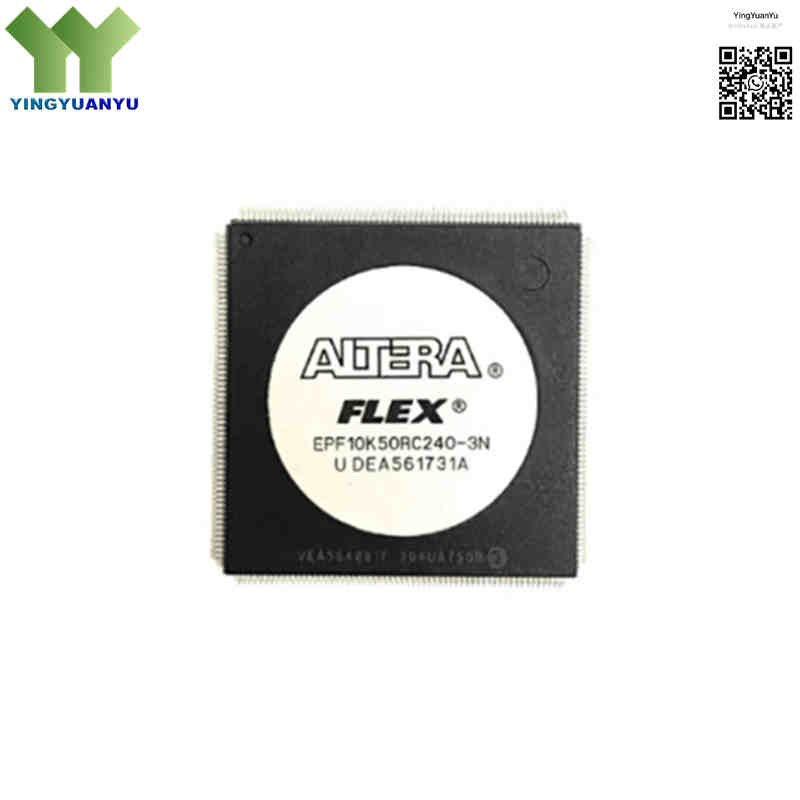
EPF10K50RC240-3N
| Part Number | EPF10K50RC240-3N |
|---|---|
| Manufacturer | Intel / Altera |
| Category | Integrated Circuits (ICs) > Embedded – FPGAs (Field Programmable Gate Array) |
| Description | FLEX 10K FPGA featuring 50,000 typical gates (116,000 maximum gates), 2,880 logic elements, 20,480 bits of embedded RAM, and 189 user I/O pins, packaged in a lead-free 240-pin RQFP outline. |
| Stock Status | In Stock |
| Origin | Original Factory |
Product Overview
The EPF10K50RC240-3N is a high-density FPGA from Altera’s classic FLEX 10K series (now Intel PSG). Equipped with 2,880 logic elements, 20,480-bit embedded RAM and up to 116,000 maximum gates, it efficiently runs complex logic and digital signal processing. Supporting 5V/3.3V multi-voltage I/O with 4.75–5.25V core voltage, this lead-free 240-pin thermally enhanced RQFP fits legacy equipment, industrial control, embedded computing and precision instrumentation.
Core Advantages
Flexible Embedded Array Architecture
Dedicated EAB blocks implement memory, DSP arithmetic and custom lookup tables directly on hardware to boost routing efficiency.
MultiVolt Mixed I/O Support
Dual 5V/3.3V signal buffers eliminate extra level-shifting chips for multi-voltage circuit boards.
Stable Fast Timing Performance
Uniform FastTrack routing delivers predictable signal delays, simplifying design simulation and timing closure.
Thermally Optimized Packaging
Built-in copper heat spreader on R suffix package improves heat dissipation under high-speed continuous operation.
Key Specifications
| Brand | Intel / Altera FLEX 10K® Programmable Logic Device Series |
|---|---|
| RoHS Status | RoHS Compliant / Lead-Free Verified (“N” suffix composition) |
| EDA/CAD Model | 3D STEP Models, Schematic symbols, and pinout footprint layout options |
| Warranty | 1-Year Standard Quality Warranty |
| Package / Case | 240-RQFP (32mm x 32mm) |
| Mounting Type | Surface Mount |
| Surface Marking / Silkscreen | EPF10K50RC240-3N Marking |
| Number of Logic Elements (LEs) | 2,880 LEs |
| Number of Logic Array Blocks (LABs) | 360 LABs |
| Total Typical / Maximum Gate Count | 50,000 Typical Gates / 116,000 Maximum Gates |
| Total Embedded RAM Bits | 20,480 Bits (Structured across 10 independent Embedded Array Blocks) |
| Number of User I/O Pins | 189 Programmable I/O Pins |
| Speed Grade Rating | -3 Speed Profile Designation (Fast propagation tier) |
| Maximum Operating Frequency | 125MHz |
| Core Logic Operating Voltage | 4.75V ~ 5.25V Nominal Core Supply Voltage |
| I/O Interface Compatibility | 5.0V and 3.3V I/O Interface Support via MultiVolt Power Configuration |
| Operating Temperature Range | 0℃ to +70℃ Commercial Ambient Temperature |
| Packaging Form | Anti-static Tray Packaging |
| Programming Interface | JTAG In-System Programmable (ISP) |
Typical Applications
- Legacy Infrastructure Maintenance, Industrial Telecommunication Protocols, and Data Switching Matrix Adapters
- High-Accuracy Real-Time Control Hardware, Substation Instrumentation Systems, and Factory Automation Controllers
- Embedded Coprocessing Expansion Blocks, Custom Interface Arbiters, and High-Speed Bus Bridges
- Military & Aerospace Equipment Lifecycle Maintenance, Avionics Simulation Hardware
- Digital Data Acquisition Boards, Scientific Imaging Hardware, and Multichannel Signal Multiplexing Matrices
Order & Shipping Info
| Minimum Order Quantity (MOQ) | 1 Piece |
|---|---|
| Shipping Time | Shipped within 1-2 business days |
| Delivery Time | 3-7 working days worldwide |
| Shipping Methods | DHL, UPS, FedEx, EMS |
| Payment Methods | T/T (Bank Transfer), PayPal, Credit Card, Western Union |
Technical Support
For datasheet, sample requests, stock check, or bulk pricing, please use the Quick Inquiry form. We will reply within 24 hours.
Frequently Asked Questions
Q1: Are EPF10K50RC240-3N original factory parts? How are they packaged?
A: All chips are 100% brand new original. We store them in anti-static trays and sealed moisture-proof bags to avoid static damage, oxidation and pin bending.
Q2: What does the suffix “N” in part number stand for?
A: “N” means lead-free terminal plating, fully RoHS compliant. It shares identical electrical performance with leaded versions.
Q3: Can this FPGA work with 3.3V power systems?
A: Core voltage needs 4.75V~5.25V supply, while its MultiVolt I/O pins support direct 3.3V connection without extra level shifters.
Q4: What software tools are used to program this FPGA?
A: Supported by Quartus II / MAX+PLUS II. Use JTAG interface with ByteBlaster/USB-Blaster for configuration. Contact us for design guides.
Q5: What’s the minimum order quantity for this model?
A: MOQ is 1 piece, small sample orders are acceptable.
Q6: How fast will you ship out the stock parts?
A: In-stock items ship within 1-2 working days after payment confirmed.
Q7: What’s the worldwide delivery lead time?
A: Global delivery takes 3-7 working days by standard logistics.
Q8: Is technical datasheet available for download?
A: Yes, official datasheet, CAD footprint and 3D STEP files can be sent on request.
Q9: How long is the warranty period of these chips?
A: We provide 1-year quality warranty for all original components.
Related Products

