
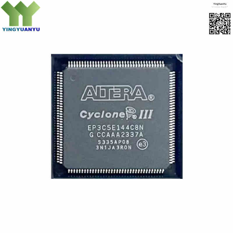
EP3C5E144C8N
| Part Number | EP3C5E144C8N |
|---|---|
| Manufacturer | Intel / Altera |
| Category | Integrated Circuits (ICs) > Embedded – FPGAs (Field Programmable Gate Array) |
| Description | Cyclone III High-Efficiency Low-Power FPGA, 5136 Logic Elements, 423Kbit Embedded RAM, 94 User I/Os, 144-Pin EQFP Package. |
| Stock Status | In Stock |
| Origin | Original Factory |
Product Overview
EP3C5E144C8N is a cost-effective low-power Cyclone III FPGA from Intel/Altera with 65nm process. It integrates 5136 LEs, 423Kbit memory and 23 multipliers, equipped with 94 multi-standard I/Os in thermal-enhanced 144-EQFP package, ideal for consumer devices, industrial control, signal bridge and display processing.
Core Advantages
65nm Low-Power Process
Adopts TSMC 65nm low-power technology to reduce static and dynamic power consumption for heat-sensitive equipment.
Embedded High-Speed DSP
Built-in 23×18-bit multipliers to deliver fast computation for filtering, modulation and control loops.
Multi-Voltage Configurable I/O Banks
Supports LVTTL, LVCMOS, LVDS and other mainstream signal standards to simplify PCB design without extra transceivers.
Heat-Optimized Package
144-pin EQFP with exposed bottom pad improves heat dissipation for stable operation under high-frequency loads.
Key Specifications
| Brand | Intel / Altera Cyclone III FPGA Series |
|---|---|
| RoHS Status | RoHS Compliant / Lead-Free Matte Tin Finish (N-Suffix Designator) |
| EDA/CAD Model | Quartus prime pin assignments, pinout libraries, and 3D step symbols available upon request |
| Warranty | 1-Year Standard Quality Warranty |
| Package / Case | LQFP-144-EP (20 mm × 20 mm) |
| Mounting Type | Surface Mount |
| Surface Marking / Silkscreen | EP3C5E144C8N Marking |
| Logic Elements (LEs) | 5,136 Logic Elements |
| Logic Array Blocks (LABs) | 321 LABs / CLBs |
| Total RAM Bits | 423,936 Bits (423 Kbit Embedded Memory Blocks) |
| Embedded Multipliers | 23 Embedded 18 × 18 Multipliers |
| Number of User I/Os | 94 I/O Pins |
| Core Supply Voltage | 1.15V to 1.25V (1.2V Nominal Core Operating Point) |
| Phase-Locked Loops (PLLs) | 2 On-Chip Global System PLLs |
| Operating Temperature Range | 0°C to +85°C (C Suffix – Commercial Grade, Speed Grade 8) |
| I/O Supply Voltage | 1.2V / 1.5V / 1.8V / 2.5V / 3.3V Multi-Voltage Support |
| Configuration Memory Type | External SPI Serial Flash (EPCS Series) |
| JTAG Interface | IEEE 1149.7 Standard JTAG Test Port |
| Storage Temperature | -65°C ~ +150°C |
| Speed Grade | 8 (Max Internal Logic Delay) |
Typical Applications
- Industrial Control Systems, Programmable Logic Controllers (PLCs), and Smart Sensor Aggregation Node Gateways
- Display Interface Bridging, High-Resolution Video Scalers, and LED Video Wall Control Matrices
- Consumer Electronic Subsystems, Smart Home Appliances, and Specialized Protocol Transceiver Interfaces
- Medical Monitoring Instrumentation, Portable Healthcare Terminals, and Diagnostic Interface Control
- Automotive Infotainment Integration, Legacy Bus Bridging, and Auxiliary Sensor Control Loops
Order & Shipping Info
| Minimum Order Quantity (MOQ) | 1 Piece |
|---|---|
| Shipping Time | Shipped within 1-2 business days |
| Delivery Time | 3-7 working days worldwide |
| Shipping Methods | DHL, UPS, FedEx, EMS |
| Payment Methods | T/T (Bank Transfer), PayPal, Credit Card, Western Union |
Technical Support
For datasheet, sample requests, stock check, or bulk pricing, please use the Quick Inquiry form. We will reply within 24 hours.
Frequently Asked Questions
Q1: What does suffix “N” on EP3C5E144C8N mean?
A: It stands for lead-free matte tin packaging, fully RoHS & WEEE compliant.
Q2: Which software supports this FPGA design?
A: Intel Quartus II / Prime (Standard/Lite edition) for synthesis and pin layout.
Q3: How to handle exposed thermal pad on PCB?
A: Solder pad to PCB copper ground plane with thermal vias for heat dissipation.
Q4: Does this chip need external flash memory?
A: Yes. It requires EPCS or SPI flash to load configuration after power reset.
Q5: What’s the operating temperature range?
A: Commercial grade 0°C ~ +85°C, storage temp: -65°C ~ +150°C.
Q6: Is EP3C5E144C8N in stock for bulk order?
A: We have spot inventory, submit inquiry for bulk discount and lead time.
Q7: Can I get free samples for testing?
A: Sample support available, fill inquiry form to apply sample quotation.
Q8: What voltage do the FPGA I/O pins support?
A: Multi-voltage I/O: 1.2V/1.5V/1.8V/2.5V/3.3V, compatible with LVDS, LVCMOS.
Related Products

