
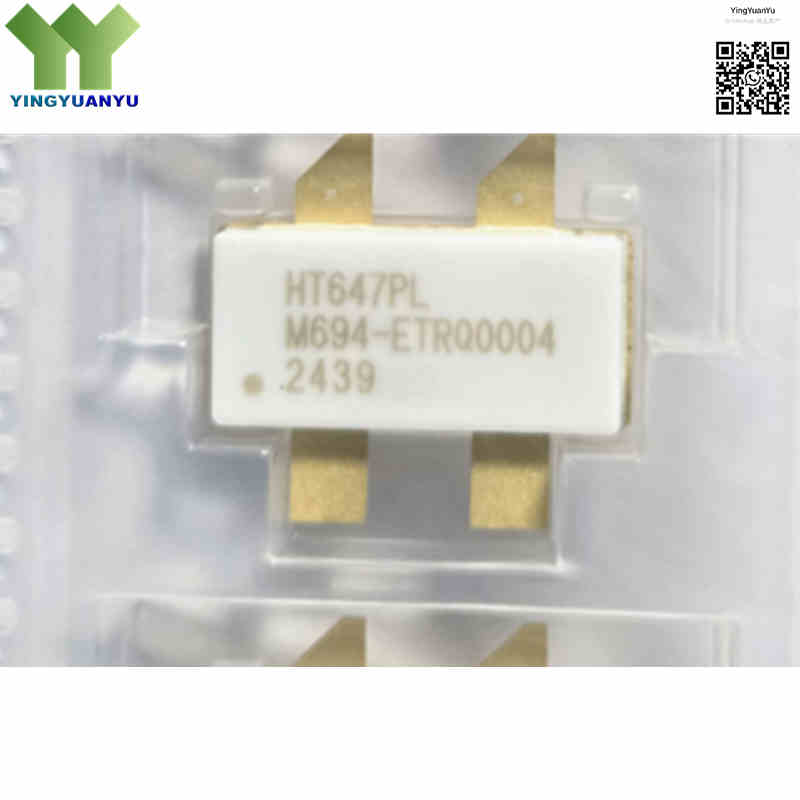
HT647PL
| Part Number | HT647PL |
|---|---|
| Manufacturer | Watech |
| Category | RF Semiconductors > RF Power LDMOS Transistors |
| Description | 200W Discrete LDMOS RF Power Amplifier, 1.8‑600MHz, For ISM Industrial & Medical RF Equipment |
| Stock Status | In Stock |
| Origin | Original Factory |
Product Overview
HT647PL is an unmatched discrete LDMOS RF power transistor, providing 200W saturated output power over 1.8‑600 MHz. It supports single‑ended and push‑pull amplifier configurations. The air‑cavity ceramic flanged package ensures low thermal resistance and high ruggedness, suitable for long‑term continuous‑wave operation in ISM industrial and medical RF equipment.
Core Advantages
High‑Power RF Performance
Delivers 200W saturated output power across 1.8‑600 MHz wide frequency bandwidth, ideal for multi‑band ISM systems.
High Efficiency & Gain
23dB power gain and 68% drain efficiency at saturation, reduces power consumption for continuous high‑power operation.
Flexible Circuit Support
Supports both single‑ended and push‑pull topologies, adapts to diverse RF power‑stage design requirements.
Superior Thermal & Robustness
Air‑cavity ceramic flange package features low thermal resistance. Good device ruggedness prevents performance degradation for long‑term industrial use.
Key Specifications
| Brand | Watech |
|---|---|
| RoHS Status | RoHS Compliant / Lead‑Free |
| EDA/CAD | Symbol, Footprint & 3D Model Available |
| Warranty | 1‑Year Standard Quality Warranty |
| Package / Case | ACC2110S-4L |
| Mounting Type | Surface Mount Device (SMD/SMT) |
| Surface Marking / Silkscreen | HT647PL Marking |
| Device Type | Discrete LDMOS RF Power Amplifier |
| Frequency Range | 1.8 MHz ~ 600 MHz |
| Operating Drain Voltage | 20 V ~ 28 V DC |
| Saturation Output Power | 200 W |
| Power Gain | 23 dB @ 28V, Ta=25℃ |
| Drain Efficiency @ Psat | 68 % |
| Circuit Configuration | Single‑ended / Push‑Pull |
| Ordering Variants | HT647PL (Reel); HT647PLB (Tray) |
| Operating Junction Temperature | -55℃ ~ +175℃ (Typical, refer to datasheet) |
| Storage Temperature Range | -65℃ ~ +175℃ |
Typical Applications
- ISM (Industrial, Scientific, Medical) RF radio‑frequency systems
- Laser generation equipment
- Plasma generation power source
- Particle accelerator RF power stage
- MRI, RF ablation and skin‑treatment medical devices
- Industrial heating, welding and drying RF power supplies
Order & Shipping Info
| Minimum Order Quantity (MOQ) | 1 Piece |
|---|---|
| Shipping Time | Shipped within 1‑2 business days |
| Delivery Time | 3‑7 working days worldwide |
| Shipping Methods | DHL, UPS, FedEx, EMS |
| Payment Methods | T/T (Bank Transfer), PayPal, Credit Card, Western Union |
Technical Support
For datasheet, sample requests, stock check or bulk pricing, please use the Quick Inquiry form. We will reply within 24 hours.
Frequently Asked Questions
Q1: What is difference between HT647PL and HT647PLB?
A: Electrical specifications are identical. HT647PL is reel‑packed, HT647PLB is tray‑packed. No difference in performance or pin‑out.
Q2: Can HT647PL work for CW continuous‑wave operation?
A: Yes, supports CW operation. Proper heatsink cooling is required to keep junction temperature within‑55℃ ~ +175℃.
Q3: Is this device pin‑to‑pin drop‑in replacement for other brand 200W LDMOS?
A: Not direct drop‑in. It is an unmatched transistor. Even if package looks similar, input‑output matching network must be re‑tuned before substitution.
Q4: What does exposed back‑side pad stand for?
A: The back flange pad is Source terminal, not ground. Do not short it to chassis ground directly without design review.
Q5: Are evaluation boards available for HT647PL series?
A: Yes, EVB reference boards: HT647PL(B)EVB and HT647PL(B)EVB1 for circuit prototype testing.
Q6: What is the recommended drain operating voltage?
A: Nominal 28 V DC, operating range 20‑28 V DC. Do not exceed maximum drain voltage rating.
Q7: What frequency range is HT647PL best‑suited for?
A: Optimal performance within 1.8 MHz‑600 MHz. Gain and efficiency will degrade outside this band.
Q8: Does HT647PL tolerate high VSWR load mismatch?
A: Limited mismatch tolerance. External protective circuit is required against high VSWR to avoid device damage.
Related Products

