
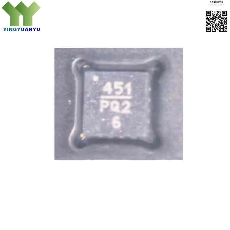
HMC451LP3ETR
| Part Number | HMC451LP3ETR |
|---|---|
| Manufacturer | Analog Devices Inc. / Hittite |
| Category | RF & Wireless > RF Amplifiers > Power Amplifiers & Gain Block MMICs |
| Description | GaAs PHEMT MMIC Medium Power Amplifier, 5 GHz‑18 GHz, 18 dB Gain(5‑16GHz),16dB Gain(16‑18GHz), 19.5 dBm P1dB, 3×3 mm QFN‑16 Exposed Pad Package. |
| Stock Status | In Stock |
| Origin | Original Factory |
Product Overview
The HMC451LP3ETR is a broadband GaAs PHEMT MMIC medium‑power amplifier from Analog Devices (Hittite). Covering 5‑18 GHz, it offers 18 dB gain(5‑16 GHz) / 16 dB gain(16‑18 GHz), +19.5 dBm P1dB and +28 dBm OIP3 from a single +5 V supply. 50‑ohm internally‑matched RF ports eliminate external matching components. Packaged in compact 3×3×0.95 mm QFN‑16, it fits point‑to‑point radio, VSAT, test instrumentation and radar systems.
Core Advantages
Broadband 5‑18 GHz Bandwidth
Wide 5‑18 GHz operating band; gain rolls‑off moderately above 16 GHz for multi‑band microwave designs.
Excellent Linear Performance
+19.5 dBm P1dB and +28 dBm OIP3, delivering low signal distortion under real‑world operating conditions.
50 Ω Internal Matching
No external RF matching networks required, simplifying PCB layout and shortening product development cycles.
High‑Performance SMT Package
QFN‑16 exposed‑pad package provides good thermal dissipation, ideal for high‑volume SMT assembly.
Key Specifications
| Brand | Analog Devices / Hittite |
|---|---|
| RoHS Status | RoHS Compliant / Green (Lead‑Free) |
| EDA / CAD | PCB Footprint & 3D Model Available upon Request |
| Warranty | 1‑Year Standard Quality Warranty |
| Package / Case | 16‑VFQFN (3×3×0.95 mm) |
| Mounting Type | Surface Mount (SMT) |
| Surface Marking / Silkscreen | 451 Marking |
| Frequency Range | 5.0 GHz to 18.0 GHz |
| Small Signal Gain | 18 dB Typ (5‑16 GHz), 16 dB Typ (16‑18 GHz) |
| Output P1dB | +19.5 dBm Typ (5‑16 GHz) |
| Saturated Output Power Psat | +21 dBm Typ (@18% PAE) |
| Output IP3 (OIP3) | +28 dBm Typ |
| Power‑Added Efficiency PAE | 18 % Typ @ Psat |
| Noise Figure | 7.0 dB Typ |
| Supply Voltage (Vdd) | +4.5 V ~ +5.5 V DC (Nominal +5.0 V DC) |
| Supply Current (Idd) | 120 mA Typ |
| Input Return Loss | ≥13 dB Typ |
| Output Return Loss | 8‑12 dB Typ |
| Input / Output Impedance | 50 Ω Internally Matched |
| Operating Temperature Range | -40°C to +85°C |
| Storage Temperature Range | -65°C to +150°C |
| ESD Rating(HBM) | Class 1A (≥250V) |
| Max Power Dissipation | 830 mW |
Typical Applications
- Point‑to‑Point and Point‑to‑Multipoint Microwave Radios
- VSAT satellite communication ground terminals and transceivers
- Test & Measurement instrumentation and RF lab signal sources
- Radar systems, electronic warfare (EW), and military communications
- LO driver amplifiers and transmitter power amplifier driver stages
Order & Shipping Info
| Minimum Order Quantity (MOQ) | 1 Piece |
|---|---|
| Shipping Time | Shipped within 1‑2 business days |
| Delivery Time | 3‑7 working days worldwide |
| Shipping Methods | DHL, UPS, FedEx, EMS |
| Payment Methods | T/T (Bank Transfer), PayPal, Credit Card, Western Union |
Technical Support
For datasheet, sample requests, stock check, or bulk pricing, please use the Quick Inquiry form. We will reply within 24 hours.
Frequently Asked Questions
Q1: What are typical applications for HMC451LP3ETR?
A: It is a 5‑18 GHz medium‑power GaAs MMIC amplifier, used as gain block or driver for microwave radio, VSAT ground terminal, test instrument, radar and LO driver circuits.
Q2: Are external RF matching components required?
A: No. RF input and output are internally 50‑Ω matched across full 5‑18 GHz bandwidth, no extra matching network needed.
Q3: What do suffix LP3 / LP3E / LP3TR / LP3ETR mean?
A: LP3 = QFN‑16 base package; “E” = lead‑free RoHS finish; “TR” = tape‑and‑reel packing. HMC451LP3ETR is lead‑free tape‑and‑reel version.
Q4: Can HMC451LP3ETR operate above 18 GHz?
A: Rated upper frequency is 18 GHz. Gain and output power degrade severely beyond 18 GHz, not recommended for 18‑20 GHz designs.
Q5: Are there direct drop‑in replacement parts?
A: No pin‑to‑pin equivalent. When selecting alternatives, confirm frequency range, gain, P1dB, supply voltage and pin‑out before redesign.
Q6: What handling precautions should I follow?
A: This is ESD‑sensitive GaAs device (HBM Class 1A). Anti‑static protection is mandatory. Exposed thermal pad must be well soldered to PCB ground plane.
Q7: Where can I get datasheet and simulation files?
A: Datasheet, S‑parameter model, PCB footprint and 3D files can be provided upon inquiry.
Related Products

