
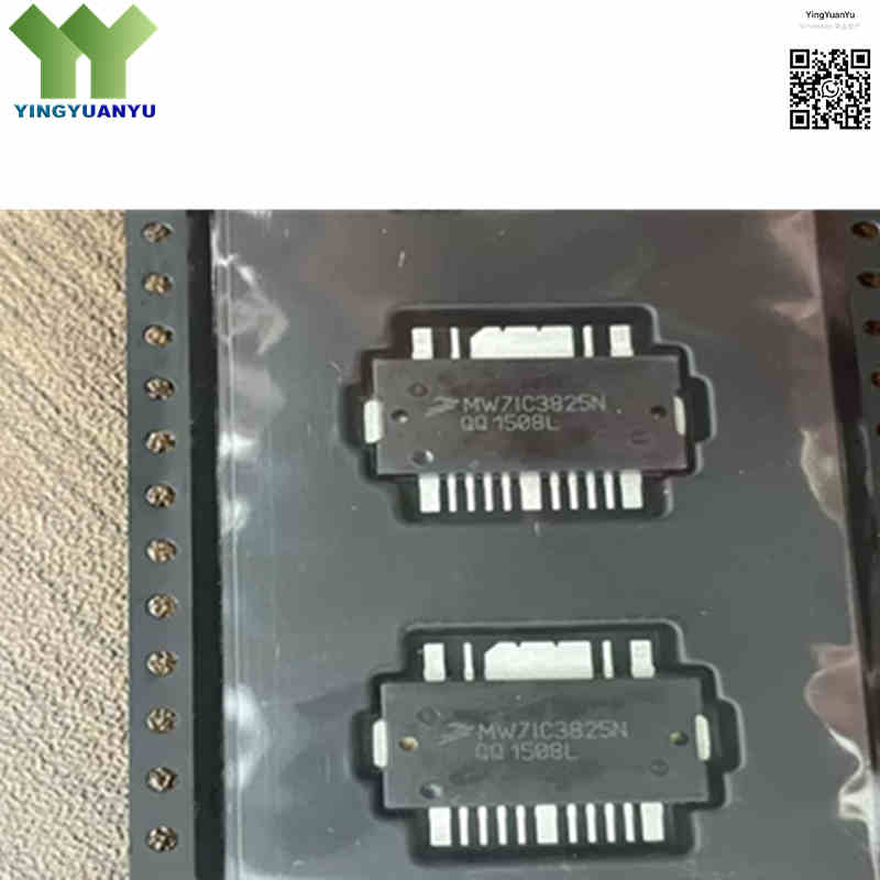
MW7IC3825NR1
| Part Number | MW7IC3825NR1 |
|---|---|
| Manufacturer | NXP Semiconductors / Freescale |
| Category | Discrete Semiconductor Products > Transistors – FETs, MOSFETs – RF |
| Description | Wideband RF Power LDMOS Integrated Transistor, 25W Avg., 3400 to 3600 MHz, 28V, TO-270-16 Package. |
| Stock Status | In Stock |
| Origin | Original Factory |
Product Overview
The MW7IC3825NR1 is a multi‑stage wideband RF power LDMOS integrated transistor from NXP (formerly Freescale). Designed for WiMAX/LTE base stations at 3400‑3600 MHz, it integrates driver & output stages with on‑chip matching. Delivers 25 W average output power at 28 V supply, with high gain, good linearity, integrated ESD protection, quiescent‑current temperature compensation and enable/disable control.
Core Advantages
High Integration
Built‑in input/output matching networks reduce external components and simplify PCB layout.
High Gain & Good Linearity
25 dB typical gain, optimized for OFDM/LTE/WiMAX complex modulation signals.
28V Optimized Performance
Optimized for 26‑32 V drain supply, delivering solid PAE to ease thermal design.
Reliable Protection & Control
TO‑270‑16 SMT plastic package with integrated ESD protection, temperature compensation and enable/disable function.
Key Specifications
| Brand | NXP Semiconductors / Freescale |
|---|---|
| RoHS Status | RoHS Compliant / Lead‑Free |
| EDA / CAD | PCB Footprint & 3D Model Available upon Request |
| Warranty | 1‑Year Standard Quality Warranty |
| Package / Case | TO‑270‑16 / OM‑780‑16 |
| Mounting Type | Surface Mount (SMD / SMT) |
| Surface Marking / Silkscreen | MW7IC3825N Marking |
| Transistor Type | RF LDMOS Multi‑Stage Power Module / Transistor |
| Frequency Range | 3400 MHz to 3600 MHz (3.4 GHz ‑ 3.6 GHz) |
| Average Output Power (Pout) | 25 W CW Avg. / 30 W @1dB Compression Point |
| Operating Drain Voltage (Vdd) | 28 V DC Typ. (26‑32V Operating Range, Max 65V Vdss) |
| Power Gain (Gps) | 25 dB Typ. @ 3500 MHz |
| Power Added Efficiency (PAE) | 15% Typ. CW; 3.5% Typ. under WiMAX/OFDM modulated signals |
| Operating Junction Temperature | -40°C to +150°C |
| Storage Temperature | -65°C to +150°C |
| Package Temperature Rating | 225°C Capable Plastic Package |
| Control Features | Integrated ESD Protection, Quiescent Current Temperature Compensation, Enable/Disable Function |
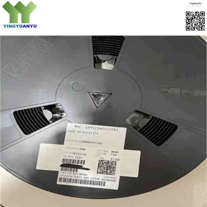
| Supply Form Factor | Tape & Reel, R1 suffix = 500 Units per reel, 44 mm Tape Width, 13 inch Reel |
Typical Applications
- WiMAX and LTE Wireless Base Station Transmitters (3.5 GHz Band)
- Broadband Wireless Access (BWA) and Fixed Wireless Infrastructure
- Point‑to‑Point and Point‑to‑Multipoint Microwave Backhaul Links
- Small Cell, Picocell, and Microcell Power Amplifier Stages
- Industrial and Commercial 3.4 ‑ 3.6 GHz RF Power Transmitters
Order & Shipping Info
| Minimum Order Quantity (MOQ) | 1 Piece |
|---|---|
| Shipping Time | Shipped within 1‑2 business days |
| Delivery Time | 3‑7 working days worldwide |
| Shipping Methods | DHL, UPS, FedEx, EMS |
| Payment Methods | T/T (Bank Transfer), PayPal, Credit Card, Western Union |
Technical Support
For datasheet, sample requests, stock check, or bulk pricing, please use the Quick Inquiry form. We will reply within 24 hours.
Frequently Asked Questions
Q1: What operating frequency band is supported by the MW7IC3825NR1?
A: Optimized for 3400 MHz‑3600 MHz (3.4‑3.6 GHz) wideband wireless applications.
Q2: What is the power output rating and operating voltage of MW7IC3825NR1?
A: Delivers 25 W CW average output power at nominal 28 V drain voltage. Operating range: 26‑32 V DC. 1 dB compression point is approx. 30 W CW.
Q3: What package style is used for MW7IC3825NR1?
A: Surface‑mount TO‑270‑16 (CASE 1886‑01) over‑molded plastic package for high power density and good thermal dissipation.
Q4: What are the differences between suffix variants: MW7IC3825NR1, MW7IC3825GNR1 and MW7IC3825NBR1?
A: All three share identical die and electrical performance. Only mechanical package differs:
• MW7IC3825NR1: Standard TO‑270‑16 (CASE 1886‑01) SMT package.
• MW7IC3825GNR1: Gull‑wing pin variant (CASE 1887‑01).
• MW7IC3825NBR1: WB‑16 variant (CASE 1328‑09).
Electrical parameters are fully interchangeable; only PCB footprint changes.
Q5: Are there direct compatible / alternative replacement parts for MW7IC3825NR1?
A: Pin‑to‑pin compatible alternatives are MW7IC3825GNR1 & MW7IC3825NBR1 (same die, different package). For other 3.4‑3.6 GHz 25 W LDMOS alternatives, please contact our sales based on your PCB footprint and thermal requirements.
Q6: Does MW7IC3825NR1 have built‑in ESD protection and control functions?
A: Yes. It features integrated ESD protection, quiescent‑current temperature compensation, enable/disable control, plus on‑chip 50 Ω input matching network.
Q7: What is the PAE performance of MW7IC3825NR1 under different signal conditions?
A: At 28 V, 3500 MHz:
• CW continuous‑wave: typical PAE = 15%
• WiMAX / OFDM modulated signal: typical PAE = 3.5%
Q8: What is the maximum VSWR withstand capability of this device?
A: The MW7IC3825NR1 can safely handle 10:1 VSWR at 32 V, 3500 MHz, 25 W CW output power.
Related Products

