
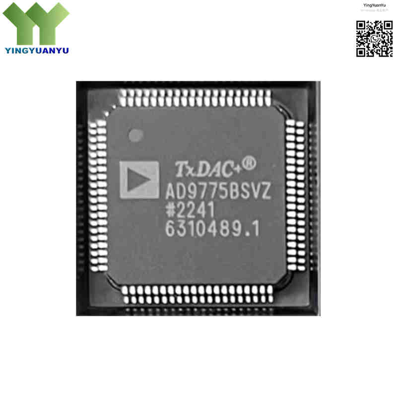
AD9775BSVZ
| Part Number | AD9775BSVZ |
|---|---|
| Manufacturer | Analog Devices Inc. (ADI) |
| Category | Integrated Circuits (ICs) > Data Acquisition – Digital to Analog Converters (DAC) |
| Description | High-performance, dual 14-bit, 160 MSPS TxDAC+ digital-to-analog converter featuring 2×/4×/8× interpolation filters, integrated complex digital modulation, and excellent SFDR performance, housed in an 80-lead TQFP_EP footprint. |
| Stock Status | In Stock |
| Origin | Original Factory |
Product Overview
The AD9775BSVZ is a dual-channel 14-bit high-speed DAC from Analog Devices TxDAC+ series. Designed for communication infrastructure, radar and test instruments, it supports up to 160 MSPS input sampling rate and reaches 400 MSPS via built-in 2×/4×/8× programmable interpolation filters. Equipped with integrated digital complex modulator and PLL clock multiplier, it realizes direct IF synthesis with consistent phase between two channels. Packaged in 80-lead TQFP-EP with exposed thermal pad, it serves as a stable signal generation chip for high-dynamic-range transmitters.
Core Advantages
Advanced Programmable Interpolation Filters
2×/4×/8× configurable hardware filters suppress out-of-band noise, reduce FPGA load and simplify external analog circuits.
Integrated Complex Digital Modulation
Built-in digital modulator supports single-sideband up-conversion, enabling direct IF output and eliminating analog quadrature imbalance.
Excellent SFDR Performance
Segmented current-source architecture delivers high spurious-free dynamic range for clean spectrum in multi-carrier communication systems.
Dual Matched High-Speed DAC Channels
Two well-matched 14-bit DAC cores offer high channel isolation and consistent phase for standard I/Q transmission designs.
Key Specifications
| Brand | Analog Devices TxDAC+ |
|---|---|
| RoHS Status | RoHS Compliant / Lead-Free / Green Manufacturing Standards Verified |
| EDA/CAD Model | 3D STEP Models, Schematic Symbols, and Pinout Footprint Configurations available upon request |
| Warranty | 1-Year Standard Quality Warranty |
| Package / Case | 80-TQFP-EP (12mm × 12mm) |
| Mounting Type | Surface Mount Technology (SMD/SMT Lead-Free Reflow Solder Line Compatibility) |
| Surface Marking / Silkscreen | AD9775BSVZ Marking |
| DAC Resolution | Dual 14-Bit Converter Channels |
| Channel Quantity | 2 Independent I/Q Channels |
| Maximum Input Data Rate | 160 MSPS (Megasamples per second) |
| Maximum Internal Clock Rate | 400 MSPS with active interpolation filters engaged |
| Interpolation Factor Selection | Bypassed (1×), 2×, 4×, or 8× selectable filters |
| Spurious-Free Dynamic Range (SFDR) | Typ. -71 dBc for 2MHz~35MHz W-CDMA bandwidth |
| Digital Interface Input Logic | Standard 3.3V CMOS Parallel Input Ports (Supports interleaved or dual-port data streaming) |
| Digital Input Voltage Level | 3.3V CMOS Logic Level |
| Analog Output Configuration | Differential Current Outputs (nominal 20 mA full-scale output current range) |
| Full-Scale Output Current | Adjustable 2mA ~ 20mA |
| Power Supplies Required | Single supply range: 3.1V ~ 3.5V for both analog & digital rails |
| Typical Power Consumption | 650mW at maximum 400MSPS operation |
| Channel-to-Channel Isolation | 65dB Typical at 100MHz |
| Clock Input Type | Single-ended or differential LVCMOS clock input |
| Operating Temperature Range | -40°C to +85°C Industrial Operating Temperature Range |
| Storage Temperature Range | -65°C to +125°C |
Typical Applications
- Cellular Base Station Transmitters, Wide-Band Communication Systems, and W-CDMA/LTE Signal Infrastructure
- Wireless Local Loop (WLL) Access Points, Point-to-Point Microwave Links, and Digital Radio Links
- High-Resolution Arbitrary Waveform Generators (AWG) and Professional RF Electronic Test Instruments
- Advanced Military Radar Waveform Synthesis, Secure Electronic Warfare (EW) Jammers, and Avionics Systems
- Direct Digital Synthesis (DDS) Systems, Ultrasound Transducer Drivers, and Broadband Signal Beamforming
Order & Shipping Info
| Minimum Order Quantity (MOQ) | 1 Piece |
|---|---|
| Shipping Time | Shipped within 1-2 business days |
| Delivery Time | 3-7 working days worldwide |
| Shipping Methods | DHL, UPS, FedEx, EMS |
| Payment Methods | T/T (Bank Transfer), PayPal, Credit Card, Western Union |
Technical Support
For datasheet, sample requests, stock check, or bulk pricing, please use the Quick Inquiry form. We will reply within 24 hours.
Frequently Asked Questions
Q1: Are AD9775BSVZ chips 100% original new?
A1: All ICs are brand new factory-original from ADI. Strict ESD & appearance inspection, shipped with original moisture-proof trays.
Q2: Why is the exposed EP pad necessary for this chip?
A2: The chip runs up to 400 MSPS and generates heat. The exposed pad provides low thermal resistance, stable performance and longer service life when soldered to PCB copper area.
Q3: How do internal interpolation filters ease FPGA load?
A3: Input data can be transmitted at low rates, while the chip internally up-samples to 400 MSPS. It cuts FPGA power consumption and simplifies peripheral filter circuits.
Q4: Can I get timing diagrams and bulk discount?
A4: Fill in our inquiry form with your project parameters and order quantity. Our engineering team will send official docs and customized quotation within one day.
Q5: What’s the lead time for AD9775BSVZ?
A5: In-stock items ship within 1-2 working days; out-of-stock orders take 2-4 weeks delivery.
Q6: Can I order small samples for testing?
A6: Yes, MOQ is 1 piece. Sample orders are supported for laboratory and prototype verification.
Q7: Do you offer after-sales replacement for defective parts?
A7: We provide 1-year warranty. Defective goods caused by manufacturing will be replaced free of charge.
Q8: Is technical consultation free during my project design?
A8: Our engineer team offers free technical support for circuit matching and parameter configuration of AD9775BSVZ.
Related Products

