
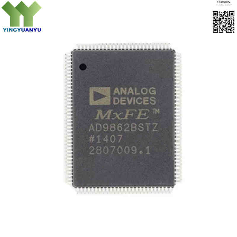
AD9862BSTZ
| Part Number | AD9862BSTZ |
|---|---|
| Manufacturer | Analog Devices Inc. (ADI) |
| Category | Integrated Circuits (ICs) > Interface – Special Purpose > Mixed-Signal Front Ends (MxFE) |
| Description | 14-Bit Mixed-Signal Front End (MxFE) Baseband Transceiver, Dual 14-Bit ADCs & Dual 14-Bit DACs, 128-LQFP Package. |
| Stock Status | In Stock |
| Origin | Original Factory |
Product Overview
The AD9862BSTZ is a high-integrated 14-bit MxFE baseband transceiver from Analog Devices. Designed for high-performance broadband communication, it integrates dual 14-bit ADCs and dual 14-bit DACs to process I/Q modulation signals. Equipped with programmable digital filters, PGA and flexible digital interface, it matches mainstream FPGA & DSP chips. Packaged in 128-pin LQFP, it delivers wide dynamic range, consistent channel matching and fixed latency, ideal for SDR, wireless local loop and cellular baseband equipment.
Core Advantages
Ultra-High Precision Mixed-Signal Architecture
Integrated matched 14-bit ADC and DAC circuits, ensuring precise phase alignment and low signal distortion for complex I/Q signal transmission.
Flexible Digital Signal Processing
Built-in 2×/4× transmit interpolation & receive decimation filters, reducing data processing load of host controllers.
On-Chip Analog Signal Conditioning
Integrated adjustable PGA and low-pass filters, cut peripheral device count and protect signal integrity.
Reliable Industrial Compatibility
Stable thermal performance, high reliability, fully compliant with global communication standards for radio and cellular access devices.
Key Specifications
| Brand | Analog Devices MxFE® Series |
|---|---|
| Part Number | AD9862BSTZ |
| RoHS Status | RoHS Compliant / Lead-Free |
| EDA/CAD Model | Schematic symbols, 3D PCB footprints, and simulation netlists are available on request |
| Warranty | 1-Year Standard Quality Warranty |
| Package / Case | 128-LQFP (14.00mm × 20.00mm) |
| Mounting Type | Surface Mount (SMT / SMD) |
| Surface Marking / Silkscreen | AD9862BSTZ Marking |
| Resolution | 14-bit (ADC & DAC) |
| Number of Channels | 2 ADC Input Channels, 2 DAC Output Channels |
| ADC Conversion Speed | Up to 64 MSPS (Dual 14-Bit Channels) |
| DAC Conversion Speed | Up to 128 MSPS (Dual 14-Bit Channels) |
| SNR (Signal-to-Noise Ratio) | 74 dB typical @ 64 MSPS ADC sampling rate |
| SFDR (Spurious-Free Dynamic Range) | 88 dB typical full-scale |
| Digital Filtering Options | 2× / 4× Interpolation; decimation, bypass modes |
| Host Communication Interface | Parallel digital I/O port interface alongside auxiliary SPI management interface |
| PGA Gain Adjustment Range | Rx PGA: -20dB ~ 0dB adjustable input gain; Tx fixed gain stages |
| Input Analog Voltage Range | 1 V p-p differential full-scale input |
| Operating Voltage (VDD) | 3.0V to 3.6V (Analog supply) / 1.8V to 3.6V (Digital interface supply) |
| Digital Logic Level | 1.8V / 3.3V compatible logic |
| Clock Input Type | Differential or single-ended reference clock input |
| Operating Temperature Range | -40°C to +70°C (Extended Commercial Grade qualification) |
| Storage Temperature Range | -65°C to +125°C |
Typical Applications
- Software-Defined Radio (SDR) platforms and military tactical transceivers
- Wireless Local Loop (WLL), point-to-point microwave communication nodes, and satellite terminals
- Broadband wireless access networks, cellular base station transceivers (BTS), and femtocells
- High-speed industrial instrumentation modems and advanced data acquisition setups
- Medical ultrasound processing pipelines and phased-array radar equipment controllers
Order & Shipping Info
| Minimum Order Quantity (MOQ) | 1 Piece |
|---|---|
| Shipping Time | Shipped within 1-2 business days |
| Delivery Time | 3-7 working days worldwide |
| Shipping Methods | DHL, UPS, FedEx, EMS |
| Payment Methods | T/T (Bank Transfer), PayPal, Credit Card, Western Union |
Technical Support
For datasheet, sample requests, stock check, or bulk pricing, please use the Quick Inquiry form. We will reply within 24 hours.
Frequently Asked Questions
Q1: What does MxFE stand for AD9862BSTZ?
A1: MxFE = Mixed-Signal Front End, ADI integrated chip series that integrates ADC, DAC and digital processing modules for transceivers.
Q2: Can Tx and Rx work with different sampling rates at the same time?
A2: Yes. Independent clock and divider circuits for transmit and receive paths support different sampling speeds as required.
Q3: What advantages does the built-in interpolation filter bring?
A3: It upsamples digital signals to raise stop-band frequency, allowing simpler, lower-cost external analog filters.
Q4: What does the suffix Z mean in AD9862BSTZ?
A4: Z stands for lead-free, fully RoHS compliant, compatible with standard wave and reflow soldering processes.
Q5: Is AD9862BSTZ in stock for spot shipment?
A5: We keep original factory stock, most orders can be shipped within 1-3 working days after payment.
Q6: Can you provide free engineering samples for testing?
A6: Yes, small sample orders are supported. Fill in the inquiry form to apply for sample pricing and quantity limits.
Q7: Which FPGA/DSP chips are compatible with this transceiver?
A7: It supports most mainstream FPGA and DSP platforms from ADI, Xilinx and TI for communication baseband design.
Q8: What is the operating temperature range of AD9862BSTZ?
A8: Extended commercial grade: -40°C to +70°C, stable for outdoor wireless communication equipment.
Q9: Does this model come with official datasheet?
A9: Original ADI datasheet is provided together with your order or sent to your email after inquiry submission.
Q10: Is bulk discount available for large quantity orders?
A10: Volume-based preferential pricing is offered for bulk purchases, contact us for customized quotation.
Related Products

