
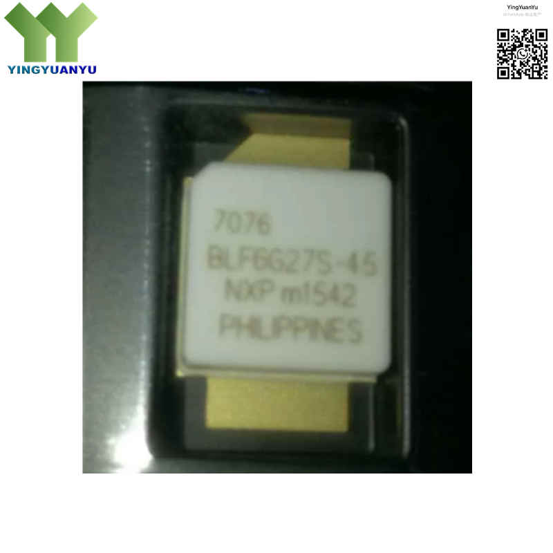
BLF6G27S‑45
| Part Number | BLF6G27S-45 |
|---|---|
| Manufacturer | Ampleon / NXP Semiconductors |
| Category | Discrete Semiconductor Products > Transistors > FETs, MOSFETs > RF FETs |
| Description | 45W LDMOS Power Transistor for Base Station Applications from 2500 MHz to 2700 MHz, SOT608B Package. |
| Stock Status | In Stock |
| Origin | Original Factory |
Product Overview
The BLF6G27S‑45 is a 45 W Gen6 LDMOS power transistor by Ampleon (formerly NXP), optimized for 2500‑2700 MHz wireless base‑station applications. It delivers high linearity, gain and efficiency for LTE/WiMAX amplifiers. Built‑in input matching and integrated ESD protection simplify circuit design. Packaged in earless ceramic SOT608B flange‑mount for superior thermal performance. Suffix “S” indicates earless package; “45” is nominal output power.
Core Advantages
Advanced Gen6 LDMOS Technology
Gen6 LDMOS delivers outstanding linearity, high gain and low thermal resistance across 2.5‑2.7 GHz.
Integrated Internal Input Matching
Built‑in input matching network simplifies PCB design and speeds up prototyping for 50‑ohm systems.
High Ruggedness & Reliability
Withstands 10:1 VSWR all‑phase load mismatch, ensuring robust operation in harsh RF environments.
Optimized Power & Linearity
Low intermodulation distortion (IMD), ideal for DPD‑enabled cellular base‑station amplifier designs.
Key Specifications
| Brand | Ampleon / NXP |
|---|---|
| RoHS Status | RoHS Compliant / Lead‑Free |
| EDA / CAD | PCB Footprint & 3D Model Available upon Request |
| Warranty | 1‑Year Standard Quality Warranty |
| Package / Case | SOT608B (Earless Flanged Ceramic Package) |
| Mounting Type | Flange Mount |
| Pin Assignment | 1‑Drain (Flange), 2‑Gate, 3‑Source |
| Surface Marking / Silkscreen | BLF6G27S‑45,Marking |
| Transistor Technology | LDMOS (Lateral Diffused Metal Oxide Semiconductor) RF Power FET |
| Frequency Range | 2500 MHz to 2700 MHz (2.5 GHz ‑ 2.7 GHz) |
| Output Power (P1dB / Peak CW) | 45 W (CW / Peak Power) |
| Average Output Power P(av) | 7 W (Single‑carrier N‑CDMA, Tcase=25°C) |
| Power Gain | Typ. 18 dB @ 2.6 GHz |
| Drain‑Source Voltage (Vdss) | 65 V DC Max (Breakdown) |
| Operating Drain Voltage (Vds) | 28 V DC Typ., Max 32 V DC |
| Quiescent Drain Current (Idq) | 350 mA (Class‑AB) |
| Threshold Voltage Vgs(th) | 1.4‑2.4 V (Id=72mA, Vds=10V) |
| Drain Efficiency ηd | Typ. 24% |
| Thermal Resistance Rth(j‑case) | 1.7 K/W (Pi=34W condition) |
| Ruggedness (VSWR) | 10:1 Load VSWR Capable (all phase angles) |
| Operating Junction Temperature | Max +200°C; Recommended ≤150°C |
| ESD Protection | Integrated internal ESD protection structure |
Typical Applications
- WiMAX, LTE, and LTE‑Advanced cellular base station power amplifiers
- Macrocell, microcell, and small cell RF transmitter driver or output stages
- W‑CDMA / UMTS wireless infrastructure equipment
- Point‑to‑point microwave communication and broadband wireless access systems
- RF industrial, scientific, and medical (ISM) amplifier modules
Order & Shipping Info
| Minimum Order Quantity (MOQ) | 1 Piece |
|---|---|
| Shipping Time | Shipped within 1‑2 business days |
| Delivery Time | 3‑7 working days worldwide |
| Shipping Methods | DHL, UPS, FedEx, EMS |
| Payment Methods | T/T (Bank Transfer), PayPal, Credit Card, Western Union |
Technical Support
For datasheet, sample requests, stock check, or bulk pricing, please use the Quick Inquiry form. We will reply within 24 hours.
Frequently Asked Questions
Q1: What is the operating frequency range of BLF6G27S‑45?
A: Optimized for 2500‑2700 MHz wireless infrastructure applications.
Q2: What is the recommended operating drain voltage?
A: Typical Vds = 28 V DC; maximum safe operating voltage is 32 V DC. Do not exceed 32 V.
Q3: What package does BLF6G27S‑45 use?
A: SOT608B earless flange‑mount ceramic package, bolt‑down mounting, non‑surface‑mount.
Q4: How to get datasheet, S‑parameters or bulk pricing?
A: Please submit an inquiry form, we will provide technical documents and quotations within 24 hours.
Q5: What are the alternative / compatible models?
A: BLF6G27‑45 (same electrical specs, with ear package, PCB footprint differs). Higher power: BLF6G27S‑60; Lower power: BLF6G27S‑30. Check datasheet before substitution.
Q6: Can BLF6G27S‑45 directly replace BLF6G27‑45?
A: Electrical performance is identical, but package mechanical size is different. Cannot swap without modifying PCB layout.
Q7: Can this transistor work outside 2500‑2700 MHz?
A: Not recommended. Gain and efficiency degrade significantly outside the rated frequency band.
Q8: What is the recommended junction temperature?
A: Max junction temp 200 °C; keep operating junction temperature ≤150 °C for long‑term reliability.
Q9: Does BLF6G27S‑45 need external matching networks?
A: Input is internally matched; external output matching network is still required for 50‑ohm system.
Related Products

