
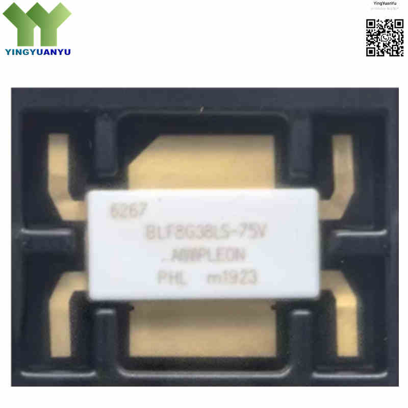
BLF8G38LS-75V
| Part Number | BLF8G38LS-75V |
|---|---|
| Manufacturer | Ampleon / NXP Semiconductors |
| Category | Discrete Semiconductor Products > Transistors – FETs, MOSFETs – RF |
| Description | Power LDMOS Transistor, 75W Peak CW, 3400 MHz to 3800 MHz, 30V, SOT1239B Package. |
| Stock Status | In Stock |
| Origin | Original Factory |
Product Overview
The BLF8G38LS‑75V is an Ampleon (formerly NXP) Gen8 LDMOS RF power transistor for 3400‑3800 MHz wireless infrastructure. It delivers 75 W peak CW output power, 20 W average power for 1‑carrier W‑CDMA signals at 30 V supply. Packaged in SOT1239B earless ceramic flange, it features internal input/output matching, high efficiency and excellent load‑mismatch ruggedness for LTE, small‑cell and Doherty power amplifier designs.
Core Advantages
Optimized High‑Frequency Performance
Gen8 LDMOS technology delivers high power density, gain and efficiency across 3.4‑3.8 GHz.
Integrated Internal Matching
Built‑in input/output matching simplifies PCB design and reduces external component count.
High Efficiency & Thermal Performance
Low‑thermal‑resistance SOT1239B package improves heat dissipation and lowers system power consumption.
High Ruggedness
Withstands VSWR 10:1 all‑phase load mismatch to protect amplifiers from unexpected reflections.
Key Specifications
| Brand | Ampleon / NXP Semiconductors |
|---|---|
| RoHS Status | RoHS Compliant / Lead‑Free |
| EDA / CAD | PCB Footprint & 3D Model Available upon Request |
| Warranty | 1‑Year Standard Quality Warranty |
| Package / Case | SOT1239B (Earless Flange Ceramic Package) |
| Mounting Type | Chassis Mount / Flange Mount |
| Surface Marking / Silkscreen | BLF8G38LS‑75V Marking |
| Transistor Type | LDMOS N‑Channel RF Power Transistor |
| Operating Frequency Range | 3400 MHz to 3800 MHz |
| Output Power (Pout) | 75 W Peak / CW Power Capabilities; 20 W average output power for 1‑carrier W‑CDMA signal |
| Drain‑Source Voltage (Vds) | 30 V DC Typ. (Max 65V Vdss) |
| Power Gain (Gps) | > 15.5 dB Typ. @ 3600 MHz |
| Drain Efficiency | > 23% (under modulated signals / high PAR); Typical 26% |
| Quiescent Drain Current (IDQ) | 600 mA Typ. @ Vds=30V |
| Gate‑Source Threshold Voltage (VGSth) | 1.9 V Typ. |
| Junction‑to‑Case Thermal Resistance (Rth(j‑c)) | 0.48 K/W Typ. |
| Thermal Resistance (Rth(j‑c)) | 0.48 K/W; Max Junction Temp: 150 °C; Storage Temp: -55 ~ 150 °C; Rated Case Temp: 80 °C |
| ESD Protection | Integrated internal ESD protection |
| Load Mismatch Ruggedness | VSWR 10:1 all‑phase operation |
Typical Applications
- LTE and WiMAX Wireless Infrastructure Base Station Power Amplifiers (3.4 GHz – 3.8 GHz)
- Sub‑6 GHz Small Cell Transmitters and Macrocell Amplifiers
- Doherty Power Amplifier Architectures and Linearized Amplifiers
- Cellular Repeater Systems and Fixed Wireless Access (FWA) Equipment
- Industrial, Scientific, and High‑Frequency Commercial RF Equipment
Order & Shipping Info
| Minimum Order Quantity (MOQ) | 1 Piece |
|---|---|
| Shipping Time | Shipped within 1‑2 business days |
| Delivery Time | 3‑7 working days worldwide |
| Shipping Methods | DHL, UPS, FedEx, EMS |
| Payment Methods | T/T (Bank Transfer), PayPal, Credit Card, Western Union |
Technical Support
For datasheet, sample requests, stock check, or bulk pricing, please use the Quick Inquiry form. We will reply within 24 hours.
Frequently Asked Questions
Q1: What frequency range does BLF8G38LS‑75V support?
A: Optimized for 3400 MHz to 3800 MHz wireless infrastructure applications.
Q2: What package is used for BLF8G38LS‑75V?
A: Earless ceramic SOT1239B flange package, delivers good thermal grounding and compact footprint.
Q3: Does BLF8G38LS‑75V have internal matching?
A: Yes. Built‑in input and output matching networks simplify circuit design and reduce external components.
Q4: What is the difference between BLF8G38LS‑75VU and BLF8G38LS‑75VJ?
A: Same die, package and electrical performance. Suffixes VU / VJ are only order‑packaging codes. This part is discontinued, only stock units are available.
Q5: Are there direct pin‑to‑pin drop‑in replacements for BLF8G38LS‑75V?
A: No direct drop‑in substitute. BLF8G38LS‑100V is the higher‑power variant with identical SOT1239B package; circuit matching and bias need re‑tuning.
Q6: Can BLF8G38LS‑75V replace BLF8G24LS‑200P / BLF8G24LS‑300P?
A: No. Those models are for 2300‑2400 MHz with SOT‑539B package. Different frequency band, package and power level, cannot interchange.
Q7: What is the difference between CW power and average power of BLF8G38LS‑75V?
A: 75 W is CW 3‑dB compression peak power; 20 W is average power under 1‑carrier W‑CDMA modulated signal for real base‑station operation. Do not mix up these two ratings in design.
Q8: What is the recommended quiescent bias current for BLF8G38LS‑75V?
A: Typical IDQ = 600 mA at Vds=30 V for class‑AB operation. Wrong bias setting will degrade linearity, efficiency or damage the device.
Q9: Is BLF8G38LS‑75V suitable for Doherty power amplifiers?
A: Yes. Low output capacitance makes it well‑suited for Doherty PA architectures.
Q10: How to get datasheet, S‑parameters or quotation for BLF8G38LS‑75V?
A: Request technical documents, stock status and volume pricing via our Quick Inquiry form, we will reply within 24 hours.
Related Products

