
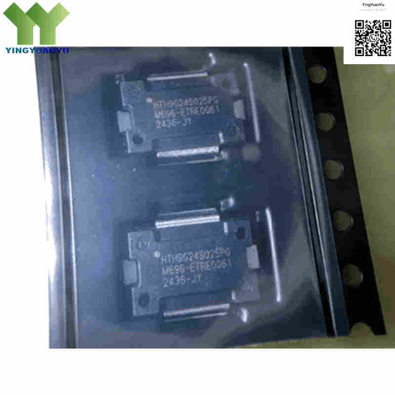
HTH9G24S025PG
| Part Number | HTH9G24S025PG |
|---|---|
| Manufacturer | Watech |
| Category | Discrete Semiconductor Products > Transistors > FETs, MOSFETs > RF MOSFETs |
| Description | Unmatched RF Power LDMOS Transistor, 0.4‑2.4 GHz, 25W Saturated Output Power, 50V Drain Operation, TO‑270‑A Package, Tape‑and‑Reel. |
| Stock Status | In Stock |
| Origin | Original Factory |
Product Overview
The HTH9G24S025PG is an unmatched N‑channel RF power LDMOS for CW and pulsed wireless communications. It delivers 25W saturated output power across 0.4‑2.4GHz at 50V nominal drain voltage. Housed in TO‑270‑A low thermal‑resistance package and supplied in tape‑and‑reel, this device features enhanced ESD protection and high load‑mismatch robustness for cellular infrastructure. External matching network is required for operation.
Core Advantages
Wide‑Band Frequency Performance
0.4‑2.4GHz wide coverage, supports multiple cellular standards and reduces part‑number inventory.
High Robustness & ESD Protection
TO‑270‑A low‑thermal‑resistance package, high VSWR tolerance and built‑in enhanced ESD protection.
50V High‑Voltage LDMOS
50V nominal drain bias with 25W saturated output power, stable performance under continuous‑wave operation.
Unmatched Discrete Device
Bare unmatched die, allows flexible external matching to optimize gain and efficiency for target bands.
Key Specifications
| Brand | Watech |
|---|---|
| RoHS Status | RoHS Compliant / Lead‑Free |
| EDA/CAD | Symbol, Footprint & 3D Model Available |
| Warranty | 1‑Year Standard Quality Warranty |
| Package / Case | TO‑270‑A |
| Mounting Type | Surface‑Mount Power Flange Package |
| Surface Marking / Silkscreen | HTH9G24S025PG Marking |
| Transistor Type | RF Power LDMOS FET, Unmatched Discrete |
| Operating Frequency Range | 0.4 GHz to 2.4 GHz |
| Saturated Output Power (Psat) | 25 W |
| Gain | 23.5 dB |
| Efficiency @ Psat | 68.3 % |
| Drain Operating Voltage (VDS) | 50 V DC Nominal |
| Operating Junction Temperature (Tj) | -65°C to +150°C |
| Packaging Format | Tape & Reel (Reel Package) |
| Production Status | MP (Mass Production) |
| Key Feature | Enhanced ESD, High VSWR Mismatch Tolerance |
Typical Applications
- CDMA Cellular Infrastructure
- W‑CDMA Base Station Driver Amplifier
- GSM EDGE & MC‑GSM RF Power Stage
- TDD / FDD LTE Wireless Communication System
- WiMAX RF Power Amplifier Modules
Order & Shipping Info
| Minimum Order Quantity (MOQ) | 1 Piece |
|---|---|
| Shipping Time | Shipped within 1‑2 business days |
| Delivery Time | 3‑7 working days worldwide |
| Shipping Methods | DHL, UPS, FedEx, EMS |
| Payment Methods | T/T (Bank Transfer), PayPal, Credit Card, Western Union |
Technical Support
For datasheet, sample requests, stock check, or bulk pricing, please use the Quick Inquiry form. We will reply within 24 hours.
Frequently Asked Questions
Q1: What does PG suffix in HTH9G24S025PG mean?
A: PG means tape‑and‑reel packing, it refers to shipping format, not physical package. Actual package is TO‑270‑A.
Q2: Is HTH9G24S025PG matched or unmatched LDMOS?
A: This is an unmatched LDMOS. External input‑output matching network is required for normal operation.
Q3: What is nominal drain supply voltage?
A: Nominal drain voltage is 50V DC. Do not exceed absolute maximum ratings to avoid device damage.
Q4: What is the difference between TO‑270‑A and TO‑270‑B?
A: Similar outline, but different pin‑out and tab dimension. TO‑270‑A cannot directly replace TO‑270‑B; PCB modification is needed.
Q5: Can HTH9G24S025PG directly replace other 25W wide‑band LDMOS?
A: It can serve as an alternative for 25W 0.4‑2.4GHz TO‑270‑A LDMOS. Pin‑out, impedance and bias differ by vendor. Re‑tune matching network; direct drop‑in replacement is not guaranteed.
Q6: Can this transistor work for 2.45GHz ISM heating?
A: Max operating frequency is 2.4GHz, not suitable for 2.45GHz ISM applications. Please select higher‑frequency RF transistor.
Q7: What key PCB layout tips for this LDMOS?
A: Keep low‑inductance grounding for flange tab, ensure good thermal dissipation, isolate input / output traces and follow datasheet absolute maximum ratings.
Q8: How can I get datasheet, S‑parameter and bulk quotation?
A: Submit your request via inquiry form. Our RF team will send related documents and volume price within 24 working hours.
Q9: What are typical gain and efficiency?
A: Typical gain 23.5 dB, drain efficiency 68.3% @ Psat. Real performance depends on PCB, matching network and operating frequency.
Related Products

