
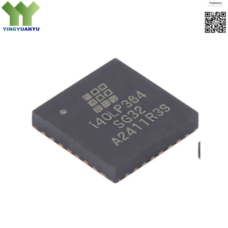
ICE40LP384-SG32
| Part Number | ICE40LP384-SG32 |
|---|---|
| Manufacturer | Lattice Semiconductor |
| Category | Integrated Circuits (ICs) > Embedded – FPGAs (Field Programmable Gate Array) |
| Description | Ultra-low power iCE40 LP Series FPGA with 384 LUTs, embedded RAM and flexible multi-voltage I/Os, compact 32-pin QFN package for IoT, mobile and handheld devices. |
| Stock Status | In Stock |
| Origin | Original Factory |
Product Overview
ICE40LP384-SG32 is Lattice’s ultra-low power FPGA from iCE40 LP series, designed for power-limited compact hardware including wearables, mobile sensors and portable diagnostic equipment. Equipped with 384 LUT logic cells and built-in non-volatile configuration memory, it delivers customizable glue logic, protocol conversion and timing control with ultra-low static & dynamic power consumption. It offloads auxiliary hardware tasks from main MCUs to extend battery life, packaged in a small QFN-32 (5x5mm) SMD housing for edge hardware acceleration.
Core Advantages
Ultra-Low Static & Dynamic Power Draw
Optimized for battery-powered devices, featuring microampere-level standby leakage to cut idle power loss of portable products.
Cost-Effective Programmable Logic
384 LUT4 logic cells plus on-chip SysMEM RAM blocks support custom state machine design without expensive ASIC development.
Multi-Voltage Configurable I/O Ports
Adjustable GPIO buffers support 1.8V/2.5V/3.3V standards, perfect for board level shifting and multi-bus signal bridging.
Complete Official Design Tool Support
Fully compatible with Lattice Radiant and iCEcube2 software, supporting fast compilation, timing verification and HDL development.
Key Specifications
| Brand | Lattice Semiconductor |
|---|---|
| RoHS Status | RoHS Compliant / Lead-Free Standard |
| EDA/CAD Model | 3D Model & PCB Footprint Available upon request |
| Warranty | 1-Year Standard Factory Warranty |
| Package / Case | QFN-32 (5x5mm) |
| Mounting Type | Surface Mount Technology (SMD/SMT) |
| Surface Marking / Silkscreen | i40LP384 SG32 Marking |
| Number of Logic Elements/Cells | 384 Look-Up Tables (LUT4 Architecture) |
| Logic Blocks / RAM Blocks | 48 Units |
| Total RAM Bits | 32768 bits Integrated SysMEM Embedded RAM |
| Number of Programmable I/Os | Up to 21 General Purpose I/O (GPIO) Pins |
| Core Voltage Supply Range | 1.14 V to 1.26 V DC (Nominal 1.2V Core Supply Rail) |
| I/O Bank Supply Voltages | Supports 1.8 V, 2.5 V, and 3.3 V Multi-Voltage Interfacing Standards |
| Configuration Type | NVCM (Non-Volatile Configuration Memory) / SPI Peripheral Master Mode Support |
| Speed Grade Descriptor | Standard Low Power Speed Grade for SG32 Package |
| Operating Temperature Range | -40°C to +100°C (Industrial/Commercial Grade Reliability Envelope) |
Typical Applications
- Smartphones, Wearable IoT Sensors, and Bio-Telemetry Health-Monitoring Rings
- Custom Protocol Translation Bridges (e.g., SPI, I2C, UART, and Customized Parallel Bus Multiplexing)
- Multi-Voltage System Level-Shifting, Custom Power-Sequencing Matrices, and Glue Logic Consoles
- LED Pattern Pulse-Width-Modulation (PWM) Controllers and Intelligent Diagnostic Indicator Hubs
- Handheld Measurement Instruments, Portable Barcode Scanners, and Remote Sensor Aggregators
Order & Shipping Info
| Minimum Order Quantity (MOQ) | 1 Piece |
|---|---|
| Shipping Time | Shipped within 1-2 business days |
| Delivery Time | 3-7 working days worldwide |
| Shipping Methods | DHL, UPS, FedEx, EMS |
| Payment Methods | T/T (Bank Transfer), PayPal, Credit Card, Western Union |
Technical Support
For datasheet, sample requests, stock check, or bulk pricing, please use the Quick Inquiry form. We will reply within 24 hours.
Frequently Asked Questions
Q1: Is your current stock inventory of the ICE40LP384-SG32 authentic factory-original parts?
A: All ICE40LP384-SG32 FPGAs are brand new original Lattice stock, stored under standard ESD and moisture control requirements to guarantee full factory performance specifications.
Q2: What does the suffix SG32 stand for in ICE40LP384-SG32?
A: SG32 refers to 32-pin 5×5mm VFQFN surface-mount package, low power standard speed grade variant for commercial & industrial temperature range.
Q3: Can this FPGA run without external flash memory?
A: Yes, it integrates built-in NVCM non-volatile memory, no external SPI flash is required for configuration after programming.
Q4: How to get PCB footprints, design files or bulk quotation?
A: Submit your demand via the inquiry form, we will send official CAD models, datasheets and volume pricing within 24 working hours.
Related Products

