
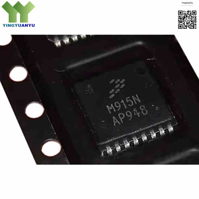
MHVIC915NR2
| Part Number | MHVIC915NR2 |
|---|---|
| Manufacturer | NXP Semiconductors / Freescale |
| Category | RF / Microwave > Integrated Circuits (ICs) > RF Power Amplifier Modules |
| Description | 15W 746–960 MHz High‑Gain Wideband LDMOS RF Integrated Power Amplifier, 26‑28V Operating Voltage, PFP‑16 Power Package. |
| Stock Status | In Stock |
| Origin | Original Factory |
Product Overview
The MHVIC915NR2 is a two‑stage wideband LDMOS RF power amplifier IC from NXP (Freescale). Operating across 746‑960 MHz with 26‑28 V supply voltage, it delivers 15 W P1dB output power with 30‑31 dB gain. This device integrates 50‑ohm input/output matching, temperature‑compensated bias, ESD protection and enable‑disable control inside PFP‑16 surface‑mount package. Optimized for GSM, EDGE, N‑CDMA base station driver and transmitter applications.
Core Advantages
Integrated Two‑stage LDMOS Architecture
Fully integrated amplifier with on‑chip RF matching network, greatly reduces external component count and PCB layout complexity.
Good Efficiency & Linearity Performance
56% PAE under GSM signal condition, excellent ACPR performance for digital cellular communication standards.
Built‑in Protection & Control Functions
Equipped with ESD protection, temperature‑compensated bias circuit and enable/disable pin for system power management.
High Anti‑VSWR Capability
Supports 3:1 full‑phase load mismatch withstand, improves field‑working reliability for radio transmitter equipment.
Key Specifications
| Brand | NXP Semiconductors / Freescale |
|---|---|
| RoHS Status | RoHS Compliant / Lead‑Free |
| EDA/CAD Resource | Symbol, Footprint & 3D Model Available |
| Warranty | 1‑Year Standard Quality Warranty |
| Package / Case | PFP‑16 Package |
| Mounting Type | Surface Mount Device (SMD/SMT) |
| Surface Marking / Silkscreen | M915N Marking |
| Technology | Silicon N‑Channel Enhancement‑Mode LDMOS RF IC |
| Frequency Range | 746 MHz to 960 MHz |
| Output Power (P1dB) | 15.0 W Typical |
| Power Gain | 30 dB (GSM), 31 dB (N‑CDMA) |
| Drain Supply Voltage | 26‑28 V DC, Typical Test Condition: 27 V DC |
| Power‑Added Efficiency (PAE) | 56% (GSM @ P1dB), 21% (N‑CDMA) |
| Quiescent Drain Current (IDQ) | 80‑120 mA(Driver Mode); 50‑140 mA(GSM Output Mode) |
| ACPR | ≤‑60 dBc (@750 kHz offset), ≤‑66 dBc (@±1.98 MHz offset) |
| VSWR Withstand Capability | 3:1 full‑phase (27V,880MHz,15W CW) |
| Thermal Resistance Rθjc | Driver stage:15.1 ℃/W; Output stage:15.8 ℃/W |
| Internal Stages | 2‑Stage Integrated Power Amplifier |
| Built‑in Features | ESD protection, Bias temperature compensation, Enable / Disable control |
| Operating Junction Temperature | -40°C ~ +150°C |
| Packaging Format | Tape & Reel (-NR2 suffix for SMT tape‑and‑reel) |
Typical Applications
- GSM, EDGE, N‑CDMA cellular base station driver & output power stage
- Sub‑1GHz wireless infrastructure, macro & micro‑cell radio transceivers
- Land Mobile Radio (LMR), public safety communication radio equipment
- 868 / 915 MHz ISM‑Band high‑power RF transmitters
- Telemetry base‑station and high‑linearity RF power modules
Order & Shipping Info
| Minimum Order Quantity (MOQ) | 1 Piece |
|---|---|
| Lead Time | Shipped within 1‑2 business days |
| Global Delivery | 3‑7 working days worldwide |
| Shipping Options | DHL, UPS, FedEx, EMS |
| Payment Methods | T/T Bank Transfer, PayPal, Credit Card, Western Union |
Technical Support
For datasheet, sample requests, stock verification or bulk quotation, please submit inquiry form. We will reply within 24 working hours.
Frequently Asked Questions
Q1: What does suffix NR2 mean for MHVIC915NR2?
A:‑N indicates RoHS lead‑free version; R2 refers to 13‑inch tape & reel for SMT automatic assembly. Its predecessor is non‑RoHS MHVIC915R2.
Q2: Are external RF matching circuits required?
A: No. 50‑ohm input/output matching is integrated on‑chip. Only low‑pass filter and DC‑block capacitors are needed on PCB.
Q3: What is the difference between driver mode and output mode?
A: Driver mode uses 27V for pre‑amplifier stage. GSM output mode runs at 26V for final transmit stage. The two modes require different quiescent‑current settings.
Q4: Are there pin‑to‑pin compatible alternative parts?
A: True pin‑to‑pin drop‑in replacements are limited. Refer to other MHVIC family devices. Send your frequency and power specs, we will suggest suitable substitutes.
Q5: How much load‑VSWR can this IC withstand?
A: It supports 3:1 full‑phase VSWR under test conditions. For field deployment, adding an isolator or circulator is strongly recommended for extra protection.
Q6: Can MHVIC915NR2 work for 915 MHz ISM‑band transmitters?
A: Yes. Its 746‑960 MHz operating range fully covers the 915 MHz ISM band. Please follow the given thermal‑resistance data for proper thermal design.
Q7: How can I get PCB layout reference and application notes?
A: Submit an inquiry form, our RF support team will send you datasheet and design reference documents.
Q8: What is the difference between MHVIC915NR2 and older MHVIC915R2?
A: They share identical electrical performance and package. MHVIC915R2 is non‑RoHS, while MHVIC915NR2 is RoHS‑compliant lead‑free variant for modern SMT production.
Related Products

