
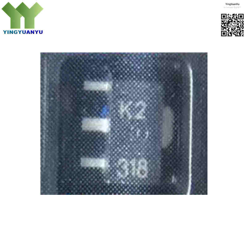
RD01MUS1-T113
| Part Number | RD01MUS1-T113 |
|---|---|
| Manufacturer | Mitsubishi Electric |
| Category | Discrete Semiconductor Products > Transistors > FETs, MOSFETs > Single RF MOSFETs |
| Description | 1W‑Class 520MHz N‑Channel Enhancement‑Mode Silicon MOSFET Transistor, 7.2V Operating Voltage, Compact SOT‑89 (R‑PSSO‑F3 / TO‑243AA) Package. |
| Stock Status | In Stock |
| Origin | Original Factory |
Product Overview
The RD01MUS1‑T113 is Mitsubishi Electric’s N‑channel enhancement‑mode RF MOSFET, optimized for VHF/UHF applications up to 520 MHz. Operating at 7.2 V supply, it delivers min 0.8 W / typical 1.4 W output power with high gain and good load ruggedness. Housed in compact SOT‑89 (R‑PSSO‑F3 / TO‑243AA) surface‑mount package, it is suitable for handheld radios, portable transceivers, wireless telemetry and RF driver amplifier circuits.
Core Advantages
High Power Gain & Drain Efficiency
Excellent VHF/UHF amplification up to 520 MHz, minimum 14 dB gain, typical drain efficiency up to 65% under 7.2 V supply.
Low‑Voltage Battery‑Powered Design
Stable operation at 7.2 V (down to 6 V input), ideal for battery‑powered portable radio and wireless devices.
Load‑Mismatch Ruggedness
Strong resistance to antenna mismatch, lowering failure risk in real‑world field usage.
Compact SMD Package
R‑PSSO‑F3 (SOT‑89 / TO‑243AA) 3‑pin small footprint, supports high‑density PCB layout.
Key Specifications
| Brand | Mitsubishi Electric |
|---|---|
| RoHS Status | RoHS Compliant / Lead‑Free |
| EDA/CAD Resources | Symbol, Footprint & 3D Model Available |
| Warranty | 1‑Year Standard Quality Warranty |
| Package / Case | SOT‑89 / TO‑243AA (R‑PSSO‑F3) |
| Mounting Type | Surface Mount Device (SMD/SMT) |
| Surface Marking / Silkscreen | K2,Marking |
| Transistor Type | N‑Channel Enhancement‑Mode RF Power MOSFET |
| Frequency Range | VHF / UHF (optimized up to 520 MHz) |
| Output Power (Pout) | Min 0.8W, Typical 1.4W (VDD=7.2V, f=520MHz, Pin=30mW) |
| Drain‑Source Voltage (VDSS) | 30 V Max |
| Gate‑Source Voltage (VGSS) | ±10 V Max |
| Drain Continuous Current (ID) | 600 mA Max |
| Total Power Dissipation (Pch) | 3.6 W |
| Power Gain (Gp) | Min 14 dB (at 520MHz, VDD=7.2V) |
| Drain Efficiency (ηD) | Typ 65% (Range 50%‑65%) |
| Junction‑to‑Case Thermal Resistance (Rth j‑c) | 34.5 °C/W |
| Gate Threshold Voltage (Vth) | 1.3 ~ 2.3 V (Typ 1.8V) |
| Operating Junction Temperature Range (Tj) | -40°C ~ +125°C |
| Pin Assignment | 1‑Gate, 2‑Source, 3‑Drain |
| Packaging Format | Tape & Reel; suffix ‑T113 defines SMT reel orientation |
Typical Applications
- Handheld two‑way radio transceivers (Walkie‑Talkie, LMR, PMR, Amateur VHF/UHF radio)
- RF driver‑stage amplifier for higher‑power RF modules
- Wireless automatic meter reading (AMR) & industrial telemetry transmitters
- Low‑power ISM‑band transmitters (433MHz, 470MHz, 500‑520MHz)
- Battery‑powered portable security & medical wireless transmission equipment
Order & Shipping Info
| Minimum Order Quantity (MOQ) | 1 Piece |
|---|---|
| Shipping Time | Shipped within 1‑2 business days |
| Delivery Lead Time | 3‑7 working days worldwide |
| Shipping Carriers | DHL, UPS, FedEx, EMS |
| Payment Options | T/T (Bank Transfer), PayPal, Credit Card, Western Union |
Technical Support
For datasheet download, sample request, stock inquiry or volume quotation, please submit inquiry via Quick Inquiry form, our RF component team will reply you within 24 hours.
Frequently Asked Questions
Q1: What does suffix ‑T113 mean for RD01MUS1‑T113?
A: ‑T113 defines tape‑and‑reel orientation for SMT pick‑and‑place. Electrical performance is identical to base RD01MUS1, only reel packaging differs.
Q2: What are key specs of RD01MUS1‑T113?
A: N‑channel RF MOSFET, 7.2V supply, min 0.8W / typ 1.4W @520MHz, ≥14dB gain,‑40℃~+125℃, SOT‑89 3‑pin SMD package.
Q3: Can RD01MUS1‑T113 work as driver for high‑power RF amplifiers?
A: Yes. With 30mW input for ~1.4W output, it is commonly used as driver/pre‑amplifier for subsequent VHF/UHF power stages.
Q4: Are there pin‑to‑pin compatible alternative parts?
A: Multiple 1W‑class SOT‑89 RF MOSFETs are available from other brands. Pin‑out, gain and thermal parameters differ, full validation is required for replacement.
Q5: Difference between SOT‑89 / TO‑243AA / R‑PSSO‑F3?
A: They refer to the same package. R‑PSSO‑F3 is Mitsubishi internal code; SOT‑89 / TO‑243AA are common industry names for this 3‑pin SMD outline.
Q6: How does it compare with other Mitsubishi small RF transistors?
A: Compared with lower‑power RD00 series, it delivers higher saturated power at 520MHz on same SOT‑89 footprint. Higher power needs larger package, cannot direct swap on PCB.
Q7: Is this part ESD‑sensitive?
A: Yes. Anti‑static handling and ESD workstation are required during assembly to avoid latent device damage.
Q8: Where to get datasheet, S‑parameter and volume price?
A: Submit inquiry via Quick Inquiry form, our RF sales team will send related documents and bulk quotation within 24 hours.
Related Products

