
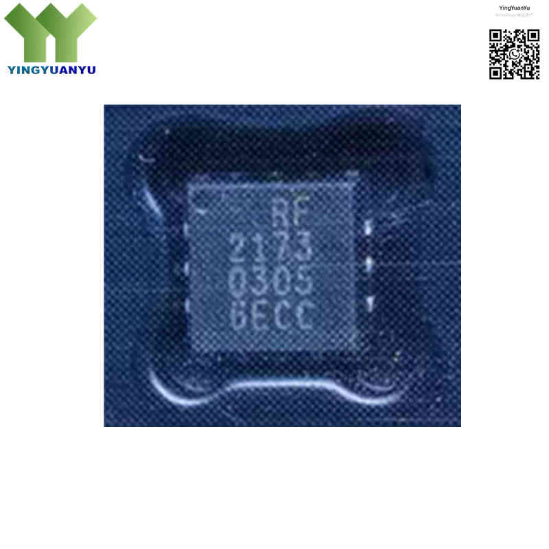
RF2173TR13
| Part Number | RF2173TR13 |
|---|---|
| Manufacturer | RFMD / Qorvo |
| Category | RF / Microwave > Integrated Circuits (ICs) > RF Power Amplifiers |
| Description | Medium‑Power RF Power Amplifier IC, 800‑950MHz, Optimized for GSM and 915MHz ISM Band, 16‑QFN Exposed‑Pad Package. |
| Stock Status | In Stock |
| Origin | Original Factory |
Product Overview
RF2173TR13 is a medium‑power RF amplifier IC from Qorvo (RFMD), optimized for 800‑950 MHz GSM and 915 MHz ISM bands. Using GaAs HBT process, it provides 30 dB typical gain @915MHz at 3.5V supply. Wide 2.7‑4.8V operating voltage fits battery‑driven and industrial radio systems. Compact 16‑QFN(16‑LCC) 4×4 mm exposed‑pad package ensures effective heat dissipation.
Core Advantages
High Gain & Efficiency
30 dB small‑signal gain; 36% PAE @P1dB, saturated PAE up to 56%, lowers power draw for radio devices.
800‑950MHz Band‑Specific Design
Tuned for GSM900 / 915MHz ISM transmit paths, perfect for sub‑1GHz industrial wireless modules.
Broad Input Voltage
2.7‑4.8V supply range (typical 3.5V), compatible with various battery and system power rails.
Thermal‑Optimized QFN Package
16‑QFN 4×4 mm exposed thermal pad, simplifies PCB thermal layout for power amplifier circuits.
Key Specifications
| Brand | RFMD / Qorvo |
|---|---|
| RoHS Status | RoHS Compliant / Lead‑Free |
| EDA/CAD | Symbol, Footprint & 3D Model Available |
| Warranty | 1‑Year Standard Quality Warranty |
| Package / Case | 16‑QFN (4mm × 4mm) |
| Mounting Type | Surface Mount Device (SMD/SMT) |
| Surface Marking / Silkscreen | RF2173 Marking |
| Technology | GaAs HBT (Heterojunction Bipolar Transistor) |
| Frequency Range | 800 MHz to 950 MHz, Optimized for GSM 915MHz ISM Band |
| Operating Voltage (Vcc) | 2.7 V ~ 4.8 V DC, Typical 3.5 V |
| Power Gain | Typ. 30 dB @ 915MHz, 3.5V Supply |
| Output Power & PAE | P1dB with 36% PAE; Saturation PAE up to 56% |
| Operating Temperature Range | -40°C to +85°C |
| Packaging Format | Tape & Reel (“TR13” denotes 13‑inch reel, 2500pcs/reel) |
| ECCN | 5A991.G |
Typical Applications
- GSM base station sub‑modules
- Industrial wireless communication equipment
- 915MHz ISM‑band RF transmit chains
- Sub‑1GHz RF power driver amplifier stages
Order & Shipping Info
| Minimum Order Quantity (MOQ) | 1 Piece |
|---|---|
| Shipping Time | Shipped within 1‑2 business days |
| Delivery Time | 3‑7 working days worldwide |
| Shipping Methods | DHL, UPS, FedEx, EMS |
| Payment Methods | T/T (Bank Transfer), PayPal, Credit Card, Western Union |
Technical Support
For datasheet, sample requests, stock check, or bulk pricing, please use the Quick Inquiry form. We will reply within 24 hours.
Frequently Asked Questions
Q1: What does suffix TR13 mean in RF2173TR13?
A: TR13 means 13‑inch tape‑and‑reel for automated SMT assembly. 2500 pieces per reel.
Q2: What is the operating voltage range for RF2173TR13?
A: Full working voltage: 2.7V‑4.8V, typical 3.5V. Do not exceed 4.8V maximum supply, or the device may get damaged.
Q3: Can RF2173TR13 work on DCS 1800MHz / PCS1900MHz bands?
A: No. This IC is optimized for 800‑950MHz GSM / 915MHz ISM. It cannot be used for 1.8‑1.9GHz cellular frequency bands.
Q4: Is an external matching circuit required for RF2173TR13?
A: Yes. Input and output RF matching networks are needed, to optimize gain, output power and efficiency for target frequency.
Q5: Are there pin‑to‑pin drop‑in alternatives for RF2173TR13?
A: No direct pin‑compatible replacement. When selecting substitutes, match frequency band, supply voltage, gain and QFN‑16 footprint. PCB re‑layout and RF re‑tuning are usually required.
Q6: What is the difference between P1dB PAE and saturated PAE?
A: 36% P1dB PAE applies for linear operation at 1‑dB compression point. Up to 56% saturated PAE works under large‑signal condition, suitable for GSM constant‑envelope modulation.
Q7: Which category should I select in store backend?
A: It is RF amplifier IC instead of discrete transistor. Choose: Integrated Circuits (ICs) > RF IC > RF Power Amplifiers.
Q8: How to implement thermal design for this 16‑QFN exposed‑pad package?
A: Connect exposed thermal pad to large PCB ground copper plane for heat dissipation. Poor thermal layout will cause power drop and overheating risk.
Related Products

