
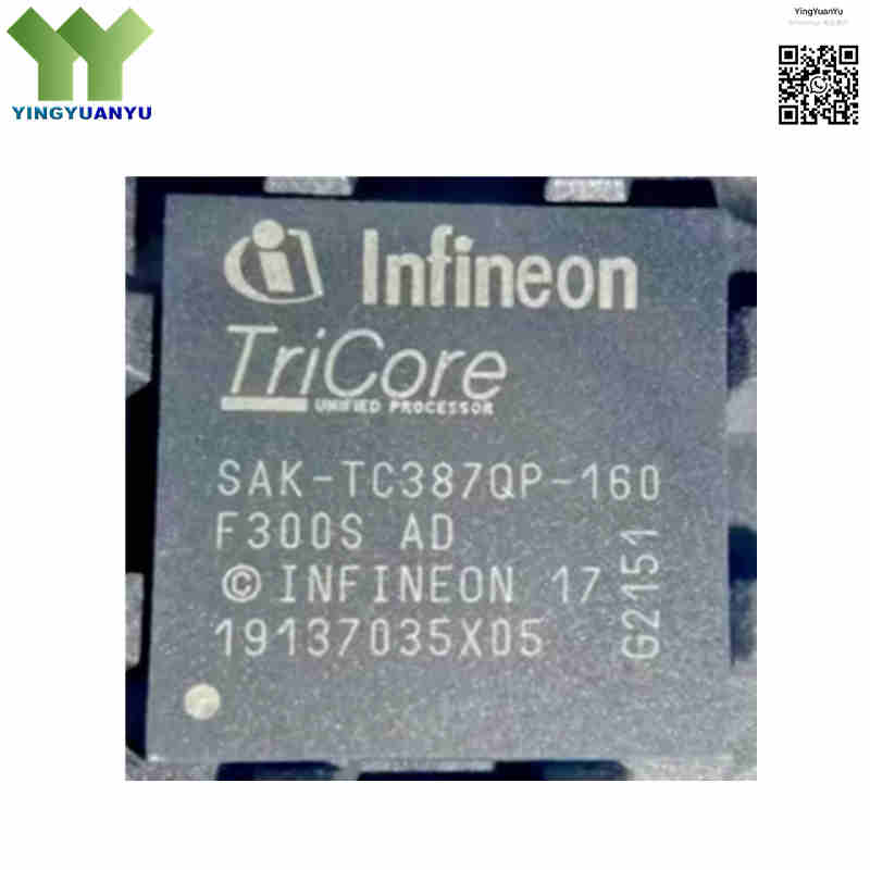
SAK-TC387QP-160F300S AD
SAK-TC387QP-160F300S AD
| Part Number | SAK-TC387QP-160F300S AD |
|---|---|
| Manufacturer | Infineon Technologies |
| Category | Integrated Circuits (ICs) > Embedded – Microcontrollers |
| Description | 32‑Bit Multi‑Core TriCore AURIX TC3xx Microcontroller, 300MHz, 10MB Flash, 1568KB SRAM, Automotive Grade (-40°C to +125°C), LFBGA‑292 Package. |
| Stock Status | In Stock |
| Origin | Original Factory |
Product Overview
The SAK‑TC387QP‑160F300S AD is a high‑performance 32‑bit automotive MCU from Infineon AURIX™ TC3xx family. It adopts quad‑core TriCore™ v1.6.2 (300 MHz, 2 lockstep cores), with 10 MB Flash and 1568 KB SRAM with ECC. Compliant with ISO 26262 ASIL‑D, it integrates EVITA‑Full HSM, Gigabit Ethernet, CAN FD, FlexRay. Packaged in LFBGA‑292, it serves for powertrain, domain controller, chassis and high‑safety automotive applications.
Core Advantages
Quad‑Core TriCore™ High‑Performance Processing
4×32‑bit TriCore™ cores up to 300 MHz, 2 lockstep cores deliver powerful real‑time computing for multi‑task automotive control.
ASIL‑D Functional Safety Compliance
Lockstep cores, MPU, bus redundancy and SMU module meet strict ISO 26262 ASIL‑D safety requirements for safety‑critical ECUs.
Large‑Capacity Embedded Memory
10 MB on‑chip Flash with ECC supports complex firmware and OTA update; 1568 KB SRAM with ECC for reliable data storage.
Advanced Security & Rich Interfaces
Built‑in EVITA‑Full HSM for vehicle security; supports Gigabit Ethernet, CAN FD, FlexRay, LIN, QSPI, SENT, PSI5 for multi‑node vehicle networking.
Key Specifications
| Brand | Infineon Technologies |
|---|---|
| RoHS Status | RoHS Compliant / Lead‑Free |
| EDA / CAD | PCB Footprint & 3‑D Model Available upon Request |
| Warranty | 1‑Year Standard Quality Warranty |
| Package / Case | LFBGA‑292 (19mm × 19mm) |
| Mounting Type | Surface Mount Device (SMD/SMT) |
| Surface Marking / Silkscreen | SAK-TC387QP-160F300S AD,Marking |
| Core Architecture | Quad 32‑Bit TriCore™ v1.6.2, 2 lockstep cores |
| Maximum CPU Speed | 300 MHz |
| Program Memory (Flash) | 10 MB On‑Chip Flash Memory with ECC |
| RAM Capacity | 1568 KB SRAM with ECC protection |
| Operating Voltage | Single‑supply: 3.3 V or 5 V (with on‑chip voltage regulator) |
| Operating Temperature | -40°C to +125°C (Standard Automotive Grade) |
| Process Technology | 40 nm |
| Safety Standard | ISO 26262 ASIL‑D / IEC 61508 SIL‑3 |
| HSM Security Module | EVITA‑Full Hardware Security Module |
| Peripherals & Interfaces | 12×CAN FD, 2×FlexRay, 24×LIN/ASCLIN, Gigabit Ethernet, 5×QSPI, 2×I2C, 25×SENT, 5×PSI5, 1×HSSL, VADC & DSADC |
Typical Applications
- Automotive Domain Controllers and Zone Control Units (ZCU)
- Advanced Driver Assistance Systems (ADAS) and Autonomous Driving Control
- Electric Vehicle (EV) Central Inverters and Powertrain Domain Managers
- Chassis Control, Advanced Active Suspension, and Braking Systems
- High‑Performance Industrial Automation and Safety Servo Controllers
Order & Shipping Info
| Minimum Order Quantity (MOQ) | 1 Piece |
|---|---|
| Shipping Time | Shipped within 1‑2 business days |
| Delivery Time | 3‑7 working days worldwide |
| Shipping Methods | DHL, UPS, FedEx, EMS |
| Payment Methods | T/T (Bank Transfer), PayPal, Credit Card, Western Union |
Technical Support
For datasheet, sample requests, stock check, or bulk pricing, please use the Quick Inquiry form. We will reply within 24 hours.
Frequently Asked Questions
Q1: What is the main difference between AURIX TC2xx and TC3xx series?
A: TC3xx delivers higher 300MHz clock speed, multi‑core architecture, larger memory, EVITA‑Full HSM and Gigabit Ethernet, outperforming the older TC2xx generation for high‑safety automotive use cases.
Q2: How many cores does SAK‑TC387QP‑160F300S AD have?
A: Quad‑core 32‑bit TriCore™ v1.6.2 running up to 300 MHz, with 2 hardware lockstep cores for ISO 26262 functional safety.
Q3: What package is used for SAK‑TC387QP‑160F300S AD?
A: LFBGA‑292 surface‑mount package, 292 balls, dimension 19 mm × 19 mm.
Q4: What does suffix “AD” stand for? What is difference vs AE variant?
A: Suffix AD = 1568 KB SRAM + full EVITA‑Full HSM. AE variant only has 1376 KB SRAM and reduced security functions. AD & AE are NOT pin‑compatible drop‑in replacements.
Q5: Are there pin‑compatible substitute models in AURIX TC3xx family?
A: SAK‑TC387QP‑160F300S‑AA is pin‑compatible with identical memory configuration. SAK‑TC387QP‑160F300S‑AE shares same package but smaller SRAM. Other TC3xx parts require hardware & firmware modification.
Q6: What are competing automotive MCUs for SAK‑TC387QP‑160F300S AD?
A: Main competitors: NXP S32K396, Renesas RH850/U2A. Both support ASIL‑D, but none are pin‑to‑pin compatible, full redesign is needed.
Q7: Does this MCU support ECC memory protection?
A: Yes, both on‑chip Flash and SRAM implement ECC error correction for safety‑critical automotive applications.
Q8: What is the difference between “QP” and “TP” suffix in AURIX TC3xx part numbers?
A: “QP” = quad‑core high‑performance variant. “TP” = dual‑core variant. Different core count and peripheral set, cannot be directly swapped.
Q9: What do the characters “160F300S” mean in the part number?
A: “160” = frequency grade; actual operating frequency is 300 MHz. “F300” denotes 300 MHz CPU clock. “S” = standard automotive temperature range (-40°C to +125°C).
Related Products

