
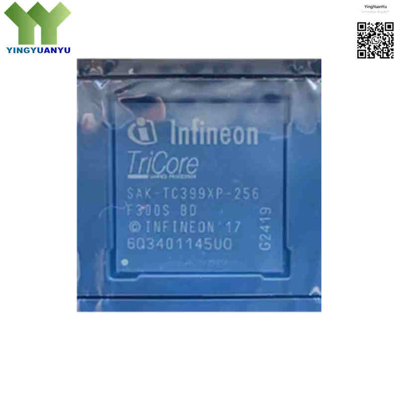
SAK-TC399XP-256F300S BD
SAK-TC399XP-256F300S BD
| Part Number | SAK-TC399XP-256F300S BD |
|---|---|
| Manufacturer | Infineon Technologies |
| Category | Integrated Circuits (ICs) > Embedded – Microcontrollers |
| Description | 32‑Bit AURIX™ TC39x Hexa‑Core TriCore™ Microcontroller, 300MHz, 16MB Flash, PG‑LFBGA‑516 Package, ASIL‑D Functional Safety. |
| Stock Status | In Stock |
| Origin | Original Factory |
Product Overview
The SAK‑TC399XP‑256F300S BD is Infineon’s flagship AURIX™ TC39x automotive MCU. It adopts a 10‑core design (6 main TriCore™ + 4 lock‑step checker cores) up to 300 MHz, with 16 MB ECC‑Flash, 6.9 MB SRAM, 1 MB EEPROM and EVITA Full HSM. Certified ISO 26262 ASIL‑D, it integrates rich automotive peripherals for domain controllers, ADAS and EV powertrain applications.
Core Advantages
10‑Core TriCore™ High‑Performance Computing
6×32‑bit TriCore™ cores plus 4 lock‑step checker cores up to 300 MHz, delivering around 4000 DMIPS for real‑time automotive control.
ASIL‑D Functional Safety
Compliant with ISO 26262 ASIL‑D, equipped with lock‑step cores, memory ECC and hardware self‑diagnosis for safety‑critical scenarios.
EVITA Full Hardware Security Module
Isolated HSM supports hardware‑accelerated cryptography, secure boot and tamper‑proof OTA firmware updates.
Rich Automotive Interfaces
Comprehensive connectivity: Gigabit Ethernet, CAN‑FD, FlexRay, LIN, QSPI, SENT, PSI5 for modern vehicle networks.
Abundant On‑Chip Peripherals
128‑channel DMA, hardware FPU, on‑chip regulator, watchdog timer and 12‑bit high‑resolution ADC for sensor acquisition.
Key Specifications
| Brand | Infineon Technologies |
|---|---|
| RoHS Status | RoHS Compliant / Lead‑Free, Halogen‑Free |
| EDA / CAD | PCB Footprint & 3D Model Available upon Request |
| Warranty | 1‑Year Standard Quality Warranty |
| Package / Case | PG‑LFBGA‑516 |
| Mounting Type | Surface Mount (SMD / SMT) |
| Surface Marking / Silkscreen | SAK-TC399XP-256F300S BD,Marking |
| Core Architecture | Hexa‑Core (6x) 32‑Bit TriCore™ v1.6.2 + 4 Lock‑Step Checker Cores, Total 10‑Core |
| Clock Speed | Up to 300 MHz |
| Program Memory (Flash) | 16 MB (with ECC protection) |
| SRAM Capacity | Up to 6.9 MB SRAM (with ECC protection) |
| EEPROM | 1 MB |
| Supply Voltage | 2.97 V ~ 5.5 V (Wide‑range single‑power supply) |
| Network Interfaces | Gigabit Ethernet, 12×CAN FD, 2×FlexRay, 12×LIN, 6×QSPI, 2×I²C, 25×SENT, 4×PSI5, 2×HSSL, 4×MSC, 1×eMMC/SDIO |
| Analog‑to‑Digital Converter | 34 ADC modules, 100‑146 channels, 12‑bit resolution |
| DMA Channels | 128‑channel DMA |
| Other Built‑in Features | Hardware FPU, On‑chip Voltage Regulator, Watchdog Timer, GTM/CCU6/GPT12 Timer Modules, EVITA Full HSM |
| Operating Temperature | -40°C to +125°C (Automotive Grade, SAK variant) |
| Functional Safety | ISO 26262 ASIL‑D / SIL‑3 |
| Certification | AEC‑Q100 Automotive Qualified |
Typical Applications
- Automotive Domain Controllers, Zone Controllers, and Central Vehicle Compute Units
- Advanced Driver Assistance Systems (ADAS) and Autonomous Driving (AD) sensor fusion nodes
- Electric Vehicle (EV) Powertrain, Main Traction Inverters, and High‑Voltage Battery Management Systems (BMS)
- Active Chassis Control, Electronic Stability Control (ESC), and Automated Braking Modules
- High‑end industrial automation, robotics controllers, and critical power electronics
Order & Shipping Info
| Minimum Order Quantity (MOQ) | 1 Piece |
|---|---|
| Shipping Time | Shipped within 1‑2 business days |
| Delivery Time | 3‑7 working days worldwide |
| Shipping Methods | DHL, UPS, FedEx, EMS |
| Payment Methods | T/T (Bank Transfer), PayPal, Credit Card, Western Union |
Technical Support
For datasheet, sample requests, stock check, or bulk pricing, please use the Quick Inquiry form. We will reply within 24 hours.
Frequently Asked Questions
Q1: How many CPU cores are in SAK‑TC399XP‑256F300S BD?
A: 10‑core architecture: 6 main 32‑bit TriCore™ cores plus 4 lock‑step checker cores, up to 300 MHz, delivering ~4000 DMIPS performance.
Q2: What is the memory configuration?
A: 16 MB ECC‑protected Flash, 6.9 MB ECC‑protected SRAM, and 1 MB on‑chip EEPROM.
Q3: What package is used for this MCU?
A: PG‑LFBGA‑516 (516‑ball surface‑mount package). Note: LFBGA‑292 is for TC397 series, not TC399XP.
Q4: What is the operating temperature range?
A: SAK variant:‑40℃~+125℃; SAL variant:‑40℃~+150℃. They are not pin‑compatible for temperature‑critical designs.
Q5: What is the difference between TC399XP and TC399XX?
A: TC399XP is the full‑feature 10‑core version. TC399XX is a 6‑core basic variant with fewer peripherals and lower computing capacity.
Q6: Are there pin‑compatible replacement parts?
A: Within AURIX TC39x family, SAK‑TC399XP‑256F300S‑BD shares pinout with other TC399XP variants (different feature sets). TC397 series uses LFBGA‑292, not pin‑compatible. No direct pin‑to‑pin drop‑in replacement from other vendors.
Q7: Does this MCU support ISO 26262 ASIL‑D functional safety?
A: Yes. It is ISO 26262 ASIL‑D / SIL‑3 qualified, with lock‑step cores, memory ECC and hardware self‑diagnosis mechanisms.
Q8: What is the power supply requirement?
A: Wide‑range single‑power supply: 2.97 V‑5.5 V, supports both 3.3 V and 5 V system power designs.
Q9: Can I use TC397XP to replace TC399XP in existing hardware?
A: No. TC397XP uses LFBGA‑292 package, while TC399XP uses PG‑LFBGA‑516. Ball count and pin assignment differ, direct hardware replacement is not allowed.
Q10: How to get datasheets, pinout details or volume quotes?
A: Request datasheets, CAD footprints, stock check and bulk pricing via our Quick Inquiry form. We will reply within 24 hours.
Related Products

