
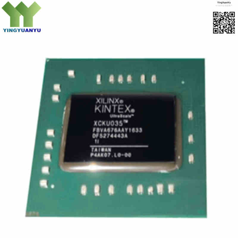
XCKU035-1FBVA676I
| Part Number | XCKU035-1FBVA676I |
|---|---|
| Manufacturer | AMD Xilinx |
| Category | Integrated Circuits (ICs) > Embedded – FPGAs (Field Programmable Gate Array) |
| Description | Kintex UltraScale FPGA featuring 444,343 Logic Cells, 19.0 Mb Total Block RAM, 312 I/O, and integrated high-speed transceivers, optimized for balance between cost, performance, and power efficiency in industrial applications. |
| Stock Status | In Stock |
| Origin | Original Factory |
Product Overview
The XCKU035-1FBVA676I is an industrial-grade FPGA from AMD Xilinx’s Kintex® UltraScale™ family. Built on a 20nm process, it delivers ASIC-class performance with 444,343 logic cells, 1,700 DSP slices, 19.0 Mb RAM, 312 I/Os, and multi-gigabit transceivers. The lead-free FCBGA-676 (27x27x1.0mm) package ensures reliability in harsh conditions, making it ideal for medical imaging, communications, machine vision, and industrial automation.
Core Advantages
ASIC-Class Kintex UltraScale Architecture
Provides exceptional system-level clocking structures and routing enhancements that boost logic utilization, maximize clock speeds, and significantly reduce execution congestion compared to legacy FPGA architectures.
Exceptional Digital Signal Processing Power
Houses 1,700 high-precision DSP slices equipped with dedicated cascade circuitry, enabling rapid, multi-channel processing of complex digital filtering, radar algorithms, and real-time beamforming tasks.
Ultra-Fast Data Interconnect and High I/O Count
Integrates ultra-low-jitter, multi-gigabit serial transceivers and a vast array of high-density parallel I/O lines, allowing effortless, low-latency interfacing with DDR4 memory arrays and standard serial buses.
Industrial-Grade Reliability and Thermal Resilience
Qualified under strict extended industrial temperature ratings, ensuring deterministic system timing, low leakage current, and stable performance inside sealed computing modules or harsh outdoor enclosures.
Key Specifications
| Brand | AMD Xilinx |
|---|---|
| RoHS Status | RoHS Compliant / Lead-Free Standard (Green Package Format) |
| EDA/CAD Model | 3D Model & PCB Footprint Available upon request |
| Warranty | 1-Year Standard Factory Warranty |
| Package / Case | FCBGA-676 (27x27x1.0mm ) |
| Mounting Type | Surface Mount Technology (SMD/SMT) |
| Surface Marking / Silkscreen | XCKU035 FBVA676 Marking |
| Family Series | Kintex® UltraScale™ |
| Logic Cells Count | 444,343 Logic Cells |
| CLB / Logic Array Blocks | 25,391 LABs/CLBs |
| Total Embedded Block RAM | 19.0 Mb (Megabits) |
| DSP Slices Array | 1,700 Computational Units |
| Number of User I/O Lines | 312 Programmable Inputs/Outputs |
| Speed Grade Tier | -1 Speed Rating Profile |
| Core Voltage Range | 0.922 V to 0.979 V DC Internal Voltage |
| Operating Temperature Range | -40°C to +100°C (Extended Industrial Thermal Junction Window) |
Typical Applications
- High-Speed Medical Imaging Systems (Ultrasound Beamforming, MRI Data Processing Cards)
- Advanced Wireless Communications (4G/5G LTE Small Cell Basestations and Remote Radio Heads)
- Industrial Machine Vision Nodes, High-Resolution Smart Cameras, and Edge AI Aggregators
- Defense and Aerospace Radar Telemetry, Secure Satellite Communications, and Guidance Controllers
- High-Frequency Electronic Test Instruments, Protocol Analyzers, and Semiconductor ATE Platforms
Order & Shipping Info
| Minimum Order Quantity (MOQ) | 1 Piece |
|---|---|
| Shipping Time | Shipped within 1-2 business days |
| Delivery Time | 3-7 working days worldwide |
| Shipping Methods | DHL, UPS, FedEx, EMS |
| Payment Methods | T/T (Bank Transfer), PayPal, Credit Card, Western Union |
Technical Support
For datasheet, sample requests, stock check, or bulk pricing, please use the Quick Inquiry form. We will reply within 24 hours.
Frequently Asked Questions
Q1: Is your stock inventory of the XCKU035-1FBVA676I guaranteed to be original and authentic?
A: Yes, we guarantee that all XCKU035-1FBVA676I FPGAs in our stock are 100% brand-new, factory-original products from AMD Xilinx, stored and handled under strict anti-static ESD shielding and humidity-controlled dry-pack standards.
Q2: What is indicated by the “I” suffix at the very end of the part number string?
A: The “I” suffix indicates an industrial-grade device. It specifies that the chip is thoroughly qualified to operate reliably across an extended junction temperature range from -40°C to +100°C, offering higher thermal resilience than a commercial-grade counterpart.
Q3: What design tools are required to program and compile bitstreams for this Kintex UltraScale device?
A: This FPGA is fully supported by AMD Xilinx’s modern Vivado® Design Suite. For optimal timing closure and area efficiency on the UltraScale architecture, it is recommended to use Vivado HLx Edition or newer releases.
Q4: How can our engineering team obtain specific pin-out spreadsheets, thermal models, or a bulk volume wholesale quotation?
A: Please complete our Quick Inquiry web form on this page with details about your processing parameters. Our application support desk will process your inquiry and dispatch the available technical documentation package within 24 hours.
Related Products

