
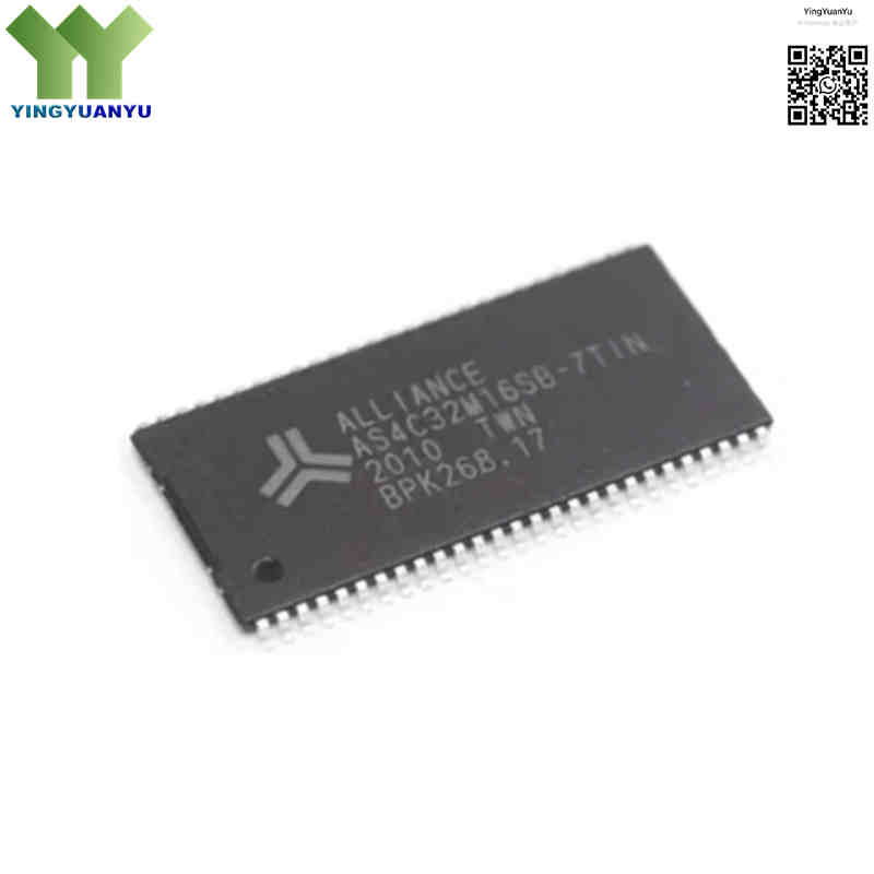
AS4C32M16SB-7TIN
| Part Number | AS4C32M16SB-7TIN |
|---|---|
| Manufacturer | Alliance Memory, Inc. |
| Category | Integrated Circuits (ICs) > Memory – SDRAM |
| Description | 512Mbit High-Speed Synchronous DRAM (SDRAM) organized as 4 Banks x 8M x 16-bit, featuring a 143MHz clock frequency, 3.0V~3.6V power supply, and industrial operating temperature range, housed in a 54-pin TSOP II package. |
| Stock Status | In Stock |
| Origin | Original Factory |
Product Overview
The AS4C32M16SB-7TIN is a high-density SDRAM from Alliance Memory. With a 512Mbit capacity structured as 4 Banks × 8M × 16-bit, it runs up to 143MHz and supports CAS latency 2/3, plus LDQM/UDQM byte mask control. Fully synchronous clock design eliminates bus skew. Packaged in 54-pin TSOP II, it meets industrial temperature standards for automotive, industrial control and network equipment.
Core Advantages
Optimized High-Speed Bandwidth
143MHz high clock frequency delivers low-latency bandwidth for video cache and network routing.
Multi-Bank Concurrent Operation
4-bank interleaving hides row precharge delay for heavy computing scenarios.
Industrial Wide Temperature Resistance
Reliable operation from -40℃ to +85℃, suitable for medical, aerospace and factory automation.
Long Product Lifecycle Support
Extended manufacturing supply avoids early component obsolescence for embedded systems.
Key Specifications
| Brand | Alliance Memory, Inc. High-Speed SDR SDRAM Family |
|---|---|
| RoHS Status | RoHS3 Compliant / Lead-Free / Green Halogen-Free Materials Verified (“N” Suffix) |
| EDA/CAD Model | 3D STEP Models, Schematic Symbols, and Pinout Footprint Configurations available upon request |
| Warranty | 1-Year Standard Quality Warranty |
| Package / Case | 54-pin TSOPII |
| Package Dimension | 10.29mm |
| Mounting Type | Surface Mount |
| Surface Marking / Silkscreen | AS4C32M16SB-7TIN Marking |
| Memory Density | 512 Mbit (536,870,912 Bits total capacity) |
| Configuration Organization | 32 Meg × 16 (4 Banks × 8,388,608 Words × 16 Bits) |
| Clock Frequency Threshold | 143 MHz Max Core Operation Frequency (-7 Speed Grade) |
| Access Time from CLK | 5.4 ns maximum data access speed at CAS Latency 3 |
| Programmable Parameters | Burst Length (1, 2, 4, 8, or Full Page) and CAS Latency (2 or 3) |
| Memory Refresh Cycle | 8K Refresh Cycles per 64 ms time interval, auto self-refresh support |
| Operating Voltage Supply | 3.0 V ~ 3.6 V Analog and Digital Signal Rail Voltages (VDD / VDDQ) |
| I/O Logic Level | LVTTL Compatible I/O Interface |
| Operating Temperature Range | -40°C to +85°C Extended Industrial Operational Limits (TA) |
| Moisture Sensitivity Level | MSL 3 (168 Hours Floor Life at 30°C / 60% RH) |
| Core Architecture | High-speed CMOS Synchronous DRAM, Concurrent Multi-Bank Operation |
| Typical Use Case | High-bandwidth embedded industrial, automotive, network communication equipment |
Typical Applications
- Industrial PLC Automation Systems, HMIs, and Edge-Compute Control Panels
- Automotive Dashboard Telematics, Rear-View Camera Buffers, and Navigation Arrays
- Commercial Networking Gateways, Cellular Base Station Routers, and Broadband Converters
- Medical Vital Sign Monitors, Diagnostic Ultrasound Hardware, and Telemetry Systems
- Consumer Electronic Media Players, High-Definition Smart Televisions, and Set-Top Boxes
Order & Shipping Info
| Minimum Order Quantity (MOQ) | 1 Piece |
|---|---|
| Shipping Time | Shipped within 1-2 business days |
| Delivery Time | 3-7 working days worldwide |
| Shipping Methods | DHL, UPS, FedEx, EMS |
| Payment Methods | T/T (Bank Transfer), PayPal, Credit Card, Western Union |
Technical Support
For datasheet, sample requests, stock check, or bulk pricing, please use the Quick Inquiry form. We will reply within 24 hours.
Frequently Asked Questions
Q1: Are AS4C32M16SB-7TIN chips 100% original new?
A1: All stock chips are genuine factory-new from Alliance Memory. We store memory components in ESD clean areas with original anti-static JEDEC trays and desiccants to avoid package cracking during reflow soldering.
Q2: What does suffix “7TIN” stand for?
A2: 7 = 143MHz speed grade, 5.4ns access time; T = 54-pin TSOP II package; I = industrial temp range -40℃~+85℃; N = lead-free RoHS3 green material.
Q3: What advantages does 32M×16 architecture bring?
A3: 16-bit bus fits ARM 16/32-bit MCUs. It doubles bandwidth vs 8-bit SDRAM and cuts PCB routing traces compared with 32-bit wide memory, lowering board cost.
Q4: What are LDQM and UDQM pins used for?
A4: They are upper/lower 8-bit data mask pins for 16-bit bus. Pull high to mask corresponding IO ports and avoid byte write/read data corruption. Contact us for timing schematic files.
Q5: What is the delivery lead time for this model?
A5: In-stock items ship within 1-2 working days; bulk large orders take 7-15 days based on quantity.
Q6: Can I get free samples for testing?
A6: Small test samples are available, just submit demands through the inquiry form with your project info.
Q7: How should I store unused SDRAM chips?
A7: Keep sealed with desiccant under MSL3 storage rules; if opened over 168 hours, bake before SMT reflow to prevent moisture damage.
Q8: Is there any compatible alternative memory chip?
A8: We offer cross-reference SDRAM models with same capacity and package, send your board specs for matching recommendation.
Related Products

