
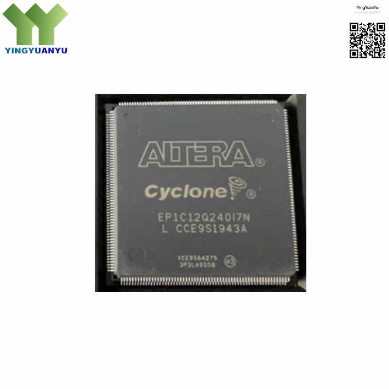
EP1C12Q240I7N
| Part Number | EP1C12Q240I7N |
|---|---|
| Manufacturer | Intel / Altera |
| Category | Integrated Circuits (ICs) > Embedded – FPGAs (Field Programmable Gate Array) |
| Description | Cyclone series industrial FPGA featuring 12,060 logic elements, 239,616 bits of embedded RAM, and 173 user I/O pins, operating at an industrial-grade speed rating within a lead-free 240-pin PQFP package. |
| Stock Status | In Stock |
| Origin | Original Factory |
Product Overview
EP1C12Q240I7N is a cost-effective, low-power industrial FPGA from Altera (Intel) Cyclone® 1 family. Built on 0.13μm full copper SRAM process, it includes 12,060 logic elements and 239,616 bits embedded M4K RAM. Rated industrial-grade (-40℃~+100℃ junction temp), this 240-pin lead-free PQFP chip fits industrial control, automotive telemetry, communication conversion and test equipment with long service life requirements.
Core Advantages
Cost-Optimized Industrial Gate Density
12,060 logic elements deliver abundant digital logic at low hardware cost for prototype and mass production.
Rugged Industrial Temperature Resistance
I-grade industrial silicon maintains stable timing and low leakage over -40℃ to +100℃ wide temperature range.
Flexible On-Chip M4K Memory
Dual-port M4K RAM blocks implement FIFO, cache and shift register functions without occupying logic resources.
Easy-to-Mount PQFP Package
240-pin gull-wing PQFP simplifies PCB layout, manual debugging and SMT assembly vs BGA packages.
Key Specifications
| Brand | Intel / Altera Cyclone® First Generation FPGA Family |
|---|---|
| RoHS Status | RoHS Compliant / Lead-Free Verified (“N” suffix composition) |
| EDA/CAD Model | 3D STEP Models, Schematic symbols, and pinout footprint layout configurations available upon request |
| Warranty | 1-Year Standard Quality Warranty |
| Package / Case | 240-PQFP (32mm x 32mm) |
| Mounting Type | Surface Mount |
| Standard Packaging Form | Anti-Static Plastic Tray |
| Surface Marking / Silkscreen | EP1C12Q240I7N Marking |
| Manufacturing Process | 0.13μm Full-Layer Copper SRAM Process |
| Number of Logic Elements (LEs) | 12,060 Logic Elements |
| Number of Logic Array Blocks (LABs) | 1,206 Independent LAB Units |
| Total Embedded RAM Bits | 239,616 Bits (Structured into 52 independent 4K M4K RAM blocks, each 4096 bits) |
| Number of User I/O Pins | 173 Programmable I/O Pins |
| I/O Feature | Hot-Swap Support Compatible |
| Supported I/O Communication Protocols | SPI, I2C, UART, Parallel Bus, Low-Speed PCI Interface |
| Number of Phase-Locked Loops (PLLs) | 2 On-Chip Advanced System PLLs for stable clock frequency multiplication and phase shifting |
| Max Internal System Clock Speed | 275MHz Maximum Internal Logic Operating Clock |
| Speed Grade Index | -7 Speed Rating Profile (Balanced industrial performance configuration tier) |
| Core Logic Supply Voltage | 1.425V to 1.575V (1.5V Nominal Core Operation Rail — VCCINT) |
| I/O Interface Voltages | Supports multi-voltage standard outputs (3.3V, 2.5V, 1.8V, 1.5V via dedicated VCCIO rails) |
| Operating Temperature Range | -40°C to +100°C Industrial Junction Temperature Limits (TJ) |
| Device Lifecycle Status | Mature Discontinued Legacy Device, Full Original Stock Available |
Typical Applications
- Industrial Automation Controllers, Programmable Logic Controllers (PLC), and Closed-Loop Motor Control Logic
- Automotive Electronics, Embedded In-Vehicle Telemetry Gateways, and Traffic Monitoring Data Recorders
- Legacy System Maintenance, Communication Protocol Converter Bridges, and Multi-Protocol Transceiver Interfaces
- Scientific Testing Instruments, Multi-Channel Digital Acquisition Boards (DAQ), and Medical Diagnostic Interfaces
- Commercial Remote Terminals, Security Access Control Hubs, and Display Driver Controller Baseboards
Order & Shipping Info
| Minimum Order Quantity (MOQ) | 1 Piece |
|---|---|
| Shipping Time | Shipped within 1-2 business days |
| Delivery Time | 3-7 working days worldwide |
| Shipping Methods | DHL, UPS, FedEx, EMS |
| Payment Methods | T/T (Bank Transfer), PayPal, Credit Card, Western Union |
Technical Support
For datasheet, sample requests, stock check, or bulk pricing, please use the Quick Inquiry form. We will reply within 24 hours.
Frequently Asked Questions
Q1: Are EP1C12Q240I7N brand new original chips?
A: All stock are 100% new original, stored in anti-static vacuum moisture-proof trays to avoid ESD damage for soldering.
Q2: What do the suffix letters I7N stand for?
A: I = industrial temp range (-40~100℃), 7 = speed grade, N = lead-free RoHS compliant package.
Q3: What’s the function of on-chip 2 PLLs?
A: PLLs multiply/divide input clock, separate core & I/O clock frequencies, reduce PCB clock jitter and peripheral parts count.
Q4: Which software can program this FPGA?
A: Intel Quartus II 13.0 SP1 is recommended; program via JTAG USB-Blaster or external EPCS serial config chip.
Q5: Is this FPGA I/O hot-swap supported?
A: Yes, the device supports hot-swap I/O, safe for live plugging peripheral modules without power cut.
Q6: What’s your MOQ and delivery time?
A: MOQ starts at 1pc, goods ship within 1-2 working days after payment.
Q7: Can you provide datasheet and CAD footprint files?
A: We offer official datasheet, 3D STEP & schematic CAD files after your inquiry.
Q8: What applications fit EP1C12Q240I7N?
A: Industrial PLC, motor control, DAQ test instruments, protocol conversion gateway and automotive circuit boards.
Related Products

