
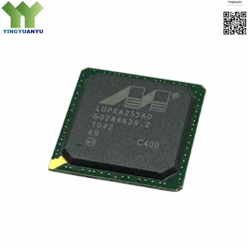
LUPXA255A0C400
| Part Number | LUPXA255A0C400 |
|---|---|
| Manufacturer | Originally designed by Intel, product line acquired by Marvell Technology Group in 2006 |
| Category | Integrated Circuits (ICs) > Embedded – Microprocessors / XScale Application Processors |
| Description | 32-Bit XScale Application Processor, 400MHz, Integrated LCD Controller and Power Management, 256-Ball PBGA Package. |
| Stock Status | In Stock |
| Origin | Original Factory |
Product Overview
The LUPXA255A0C400 is a highly integrated 32-bit embedded processor based on Intel XScale® architecture, running at 400MHz. Optimized for industrial terminals and portable POS devices, it balances performance and low power. Integrated LCD controller, memory management unit and multiple serial interfaces are built-in. Dynamic voltage scaling and low-power modes extend battery life. Packaged in 256-ball PBGA, it delivers stable long-term operation for embedded systems.
Core Advantages
High Efficiency XScale ARM v5TE Core
400MHz 32-bit RISC core with MAC DSP acceleration, fast for multimedia and embedded computing.
Multi-level Power Management
Idle/Standby/Sleep modes plus dynamic frequency scaling, reducing heat and power consumption.
On-Chip LCD Display Controller
Supports STN/TFT screens, saves extra external graphics chip and bus bandwidth.
Rich Peripheral Interfaces
Equipped with USB device, AC97/I2S audio, multi-channel UART and DMA engine for efficient data transmission.
Key Specifications
| Brand | Intel / Marvell PXA Application Processor Series |
|---|---|
| RoHS Status | Lead-Free Option / Compliant Variation Layout Available |
| EDA/CAD Model | Schematic symbols, 3D BGA package models, and 256-pin land patterns are available on request |
| Warranty | 1-Year Standard Quality Warranty |
| Package / Case | 256-PBGA (17.00 mm × 17.00 mm × 1.70 mm, pitch 1mm) |
| Mounting Type | Surface Mount (SMT / SMD Re-flow) |
| Surface Marking / Silkscreen | LUPXA255A0 C400 Marking |
| Core Architecture | 32-Bit XScale RISC Core (ARM v5TE Compliant) |
| Maximum Clock Frequency | 400 MHz |
| Data Bus Width | 32 Bit |
| Address Bus Width | 26 Bit |
| Cache Structure | 32 KB Instruction Cache / 32 KB Data Cache / 2 KB Mini-Data Cache |
| Memory Controller Support | 16-Bit or 32-Bit Synchronous DRAM (SDRAM), Flash, SRAM, PCMCIA / CompactFlash |
| Integrated Visual Engine | Dual display buffer LCD controller (Supports up to 16-bit color TFT matrix) |
| Serial Communication Ports | 3 × UART, USB 1.1 Device, I2C, SPI, AC97 / I2S audio interface codecs |
| Boundary Scan Test | Support JTAG debugging interface |
| Operating Core Voltage (VCC_CORE) | 1.3V typical at 400 MHz processing frequency |
| Operating I/O Voltage (VCC_IO) | 2.5V or 3.3V dual interface buffer tolerance matching network |
| Operating Temperature Range | 0°C to +70°C (Commercial / Extended industrial -40℃~85℃ versions optional) |
Typical Applications
- Legacy enterprise Handheld Data Terminals (HDT) and rugged barcode scanner instrumentation
- Portable Point-of-Sale (POS) electronic payment machinery and smart card validation readers
- Industrial control system display nodes, human-machine interfaces (HMI), and factory automation panels
- Embedded GPS telematics computers, transportation blackboxes, and mobile surveying machinery
- Medical telemetry monitors, portable diagnostic instruments, and laboratory sensor nodes
Order & Shipping Info
| Minimum Order Quantity (MOQ) | 1 Piece |
|---|---|
| Shipping Time | Shipped within 1-2 business days |
| Delivery Time | 3-7 working days worldwide |
| Shipping Methods | DHL, UPS, FedEx, EMS |
| Payment Methods | T/T (Bank Transfer), PayPal, Credit Card, Western Union |
Technical Support
For datasheet, sample requests, stock check, or bulk pricing, please use the Quick Inquiry form. We will reply within 24 hours.
Technical Support
For datasheets, samples, stock & bulk price, submit inquiry form, we reply within 24 hours.
Frequently Asked Questions
Q1: What does C400 mean in LUPXA255A0C400?
A: C400 means this chip supports max 400MHz operation under 1.3V core voltage.
Q2: Can it run standard ARM software?
A: Yes, fully compatible with ARM v5TE. Supports ARM compiler, embedded Linux & WinCE.
Q3: What flash storage can this chip connect?
A: Supports parallel NOR Flash, asynchronous SRAM and multi-burst flash without extra glue circuit.
Q4: How does LCD controller save power?
A: Built-in DMA reads display data directly from SDRAM, reducing frequent CPU wake-up and power loss.
Q5: Can I get free samples of LUPXA255A0C400?
A: We provide small quantity samples, you only need to cover shipping cost via inquiry form.
Q6: What’s the normal lead time for bulk orders?
A: Standard stock items ship within 1-2 working days.
Q7: What package is LUPXA255A0C400?
A: 256-PBGA, size 17×17×1.7mm, ball pitch 1mm, JEDEC code S-PBGA-B256.
Q8: Are industrial wide-temperature versions available?
A: This model is commercial grade (0~70℃); industrial -40~85℃ versions are optional upon request.
Q9: What development tools match this processor?
A: Standard ARM JTAG debugger, Linux SDK and evaluation boards are available for development.
Related Products

