
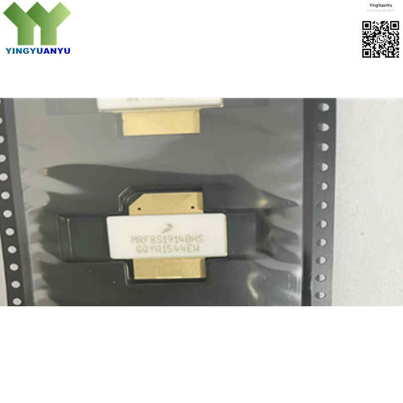
MRF8S19140HS
| Part Number | MRF8S19140HS |
|---|---|
| Manufacturer | NXP Semiconductors / Freescale |
| Category | Discrete Semiconductor Products > Transistors > FETs, MOSFETs > RF MOSFETs |
| Description | 140W Peak RF Power LDMOS Transistor, 1930 to 1990 MHz, 28V, NI‑780S Package, Obsolete. |
| Stock Status | In Stock |
| Origin | Original Factory |
Product Overview
The MRF8S19140HS is a high‑power N‑Channel LDMOS RF power transistor from NXP (formerly Freescale). Optimized for 1930‑1990 MHz base‑station applications, it delivers 140 W peak / 34 W average output power under W‑CDMA/LTE modulation at 28 V supply. Featuring integrated input & output matching and built‑in ESD protection, it provides high gain and good linearity for wireless infrastructure. This part is officially discontinued (Obsolete).
Core Advantages
High Power Density & Linearity
Delivers 140 W peak output at 28 V, with high gain and excellent linearity for multi‑carrier W‑CDMA / LTE cellular systems.
Integrated Matching & ESD Protection
Built‑in input and output matching simplifies circuit design; integrated ESD protection improves assembly reliability.
Effective Thermal Dissipation
NI‑780S earless flange package with low thermal resistance ensures stable heat dissipation under continuous high‑power operation.
High Efficiency Performance
Typical PAE exceeds 30% under modulated signals, lowering power consumption and thermal load.
Key Specifications
| Brand | NXP Semiconductors / Freescale |
|---|---|
| RoHS Status | RoHS Compliant / Lead‑Free |
| EDA / CAD | PCB Footprint & 3D Model Available upon Request |
| Warranty | 1‑Year Standard Quality Warranty |
| Package / Case | NI‑780S (Earless Flange Package) |
| Mounting Type | Flange Mount |
| Surface Marking / Silkscreen | MRF8S19140HS Marking |
| Transistor Type | N‑Channel RF LDMOS FET |
| Operating Frequency | 1930 MHz to 1990 MHz |
| Continuous Power Output (Pout) | 140 W Peak / 34 W Average (W‑CDMA / LTE) |
| Power Gain (Gp) | > 18 dB Typ. (@ 1960 MHz, 28V) |
| Operating Drain Voltage (Vdd) | 28 V DC Typ. (Max 32V) |
| Drain‑Source Breakdown Voltage (Vbr)dss | 65 V DC Min |
| Gate‑Source Breakdown Voltage (VGS) | ±10 V (Max Negative ‑6 V, Positive +10 V) |
| Quiescent Drain Current (IDQ) | 1100 mA Typical |
| 1 dB Compression Point | ≈138 W CW |
| VSWR Ruggedness | 10:1 Mismatch Tolerance (32V, 1960 MHz) |
| Thermal Resistance (RθJC) | 0.48 °C/W (@34 W); 0.45 °C/W (@140 W) |
| Operating Junction Temperature (TJ) | +150°C Max |
| Storage Temperature | -65°C to +150°C |
| Product Status | Obsolete / Discontinued |
Typical Applications
- 3G / 4G / LTE cellular infrastructure base station power amplifiers
- W‑CDMA, UMTS, and GSM/EDGE transmitter power amplifier stages
- Doherty high‑efficiency power amplifier architectures
- Microcell and macrocell wireless telecommunication transmitters
- Industrial RF generators and power amplifiers in the 1.9 GHz frequency band
Order & Shipping Info
| Minimum Order Quantity (MOQ) | 1 Piece |
|---|---|
| Shipping Time | Shipped within 1‑2 business days |
| Delivery Time | 3‑7 working days worldwide |
| Shipping Methods | DHL, UPS, FedEx, EMS |
| Payment Methods | T/T (Bank Transfer), PayPal, Credit Card, Western Union |
Technical Support
For datasheet, sample requests, stock check, or bulk pricing, please use the Quick Inquiry form. We will reply within 24 hours.
Frequently Asked Questions
Q1: What frequency band is the MRF8S19140HS designed for?
A: Optimized for 1930‑1990 MHz (PCS / 1.9 GHz) wireless communication band.
Q2: What is the recommended operating supply voltage?
A: Typical Vdd = 28 V DC; maximum continuous supply is 32 V.
Q3: What package does MRF8S19140HS adopt?
A: Earless ceramic NI‑780S flange package (Case 465a‑06 Style 1), low thermal resistance for high‑power operation.
Q4: How to get datasheet, S‑parameters or volume pricing?
A: Request datasheets, evaluation files, stock check and bulk pricing via our Quick Inquiry form.
Q5: What do suffixes HS, R5, R3 mean?
A: HS = single‑unit NI‑780S flange package. R5/R3 are tape‑and‑reel variants. Electrical performance is identical.
Q6: Is MRF8S19140HS a surface‑mount device?
A: No. It is flange‑mount, requires screw‑mounting onto heat sink.
Q7: Does it support Doherty amplifier topology?
A: Yes, suitable for Class‑AB / C and Doherty PA designs for cellular base stations.
Q8: What are the replacement parts for this obsolete model?
A: MRF8S19140HS is discontinued. Contact our team for 1930‑1990 MHz compatible alternatives. Note: circuit redesign is required for replacements.
Q9: Does it have built‑in input & output matching?
A: Yes. Internal matching networks are integrated for typical application circuits.
Q10: What is maximum junction temperature?
A: Max Tj = +150°C. Proper heat‑sinking is mandatory for continuous high‑power use.
Related Products

