
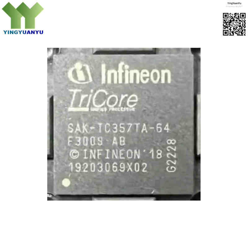
SAK-TC357TA-64F300S AB
SAK-TC357TA-64F300S AB
| Part Number | SAK-TC357TA-64F300S AB |
|---|---|
| Manufacturer | Infineon Technologies |
| Category | Integrated Circuits (ICs) > Embedded – Microcontrollers |
| Description | 32‑Bit TriCore™ AURIX™ TC35xTA ADAS Microcontroller, 300 MHz, 4 MB Mirrored‑Bank Flash, ISO 26262 ASIL‑D Compliant, LFBGA‑292 Package. |
| Stock Status | In Stock |
| Origin | Original Factory |
Product Overview
The SAK‑TC357TA‑64F300S AB is a high‑performance 32‑bit automotive ADAS MCU from Infineon AURIX™ TC35xTA family. It features 3×TriCore™ v1.6.2 cores (2 lockstep cores) @300 MHz, 4 MB mirrored‑bank Flash, 3.52 MB ECC‑protected SRAM with dedicated radar RAM. Equipped with dual SPU radar accelerators and EVITA‑Full HSM, it meets ISO 26262 ASIL‑D. Packaged in LFBGA‑292, suffix AB denotes tape‑and‑reel AB‑step enhanced revision. Ideal for automotive radar and ADAS domain control.
Core Advantages
Triple TriCore™ v1.6.2 with Dual Lockstep Cores
3×TriCore™ v1.6.2 @300 MHz, 2 lockstep cores deliver real‑time performance for radar signal processing.
ISO 26262 ASIL‑D Functional Safety
Full ECC memory protection & hardware self‑test simplify ASIL‑D certification for safety‑critical automotive systems.
Dual SPU Radar Hardware Accelerators
2×SPU units handle FFT/CFAR operations, off‑loading heavy millimeter‑wave radar computing from main CPUs.
EVITA‑Full HSM Security Module
Hardware‑accelerated crypto, secure boot and anti‑tamper protection support secure OTA firmware updates.
Rich Automotive Peripherals
8×CAN‑FD, Gigabit Ethernet, FlexRay, 4×LIN, 4×QSPI, 64‑channel DMA, RTC & FPU for ADAS system integration.
Key Specifications
| Brand | Infineon Technologies |
|---|---|
| RoHS Status | RoHS Compliant / Lead‑Free, RoHS 3.0 |
| EDA / CAD | PCB Footprint & 3D Model Available upon Request |
| Warranty | 1‑Year Standard Quality Warranty |
| Package / Case | LFBGA‑292 (17mm×17mm, 292 balls) |
| Mounting Type | Surface Mount (SMD / SMT) |
| Surface Marking / Silkscreen | SAK-TC357TA-64F300S AB,Marking |
| Core Architecture | Triple 32‑Bit TriCore™ v1.6.2 Architecture (2 lockstep cores) |
| Max Clock Speed | 300 MHz |
| Program Memory Size | 4 MB Flash (Mirrored Bank A/B Swap) |
| RAM Capacity | 3.52 MB SRAM (3520 KB, ECC‑protected, includes dedicated radar‑RAM) |
| Connectivity | Gigabit Ethernet, 8×CAN‑FD, FlexRay, 4×LIN, 4×QSPI, I²C, UART |
| Hardware Accelerators | 2×SPU (FFT / CFAR radar acceleration), EVITA‑Full HSM |
| Supply Voltage | 3.3V ±10% or 5V ±10% (on‑chip voltage regulator supported) |
| Operating Temperature | -40°C to +125°C (Automotive Grade TA) |
| Peripheral Features | 64‑channel DMA, Watchdog timer, RTC, Floating‑Point Unit (FPU), 2×ADC modules |
| Functional Safety | ISO 26262 ASIL‑D / IEC 61508 SIL‑3 |
Typical Applications
- Automotive millimeter‑wave radar (long‑range / mid‑range radar)
- ADAS domain controller, radar‑camera fusion modules
- Electric vehicle powertrain control, inverter & BMS
- Automotive transmission control, chassis domain control
- High‑safety industrial motion control and robotics
Order & Shipping Info
| Minimum Order Quantity (MOQ) | 1 Piece |
|---|---|
| Shipping Time | Shipped within 1‑2 business days |
| Delivery Time | 3‑7 working days worldwide |
| Shipping Methods | DHL, UPS, FedEx, EMS |
| Payment Methods | T/T (Bank Transfer), PayPal, Credit Card, Western Union |
Technical Support
For datasheet, sample requests, stock check, or bulk pricing, please use the Quick Inquiry form. We will reply within 24 hours.
Frequently Asked Questions
Q1: What is the core configuration of SAK‑TC357TA‑64F300S AB?
A: Triple‑core TriCore™ v1.6.2 (2 lockstep cores), 300 MHz, 4 MB mirrored‑bank Flash, 3.52 MB SRAM with dedicated radar RAM, dual SPU radar accelerators integrated.
Q2: What does suffix AB stand for? What is the difference between AB‑step and older step versions?
A: AB means tape‑and‑reel packaging. AB‑step is enhanced revision with improved safety & stability. Refer to Infineon errata sheet for hardware notes. Tube‑packaged variant uses suffix AA; AB‑step is recommended for new projects.
Q3: Are there pin‑compatible models within AURIX TC35xTA family?
A: SAK‑TC357TA‑48F300S AB and SAK‑TC357TA‑80F300S AB share LFBGA‑292 pin‑out. Flash sizes differ: 48F=3MB, 64F=4MB, 80F=5MB. Check datasheet before direct substitution.
Q4: What are the main differences between SAK‑TC357TA‑64F300S AB and SAK‑TC375TA‑64F300S AB?
A: Both use LFBGA‑292, same 3‑core TriCore v1.6.2 & 4 MB Flash. TC375TA adds more high‑speed interfaces. TC357TA is radar‑optimized with dedicated SPU accelerators for cost‑effective radar‑focused ADAS designs.
Q5: Can other‑brand automotive MCUs be used as cross‑brand alternatives?
A: NXP S32K396 and Renesas R‑Car S3 are functional alternatives for ADAS domain control, supporting ASIL‑D safety. They lack dedicated SPU radar accelerators. Software & peripheral mapping must be reworked, no pin‑to‑pin replacement.
Q6: What is the package difference between LFBGA‑292 and other BGA variants in TC35xTA series?
A: LFBGA‑292 is 17×17mm full‑feature BGA. Lower‑end variants adopt LFBGA‑208 with fewer balls, reduced peripherals and smaller memory. LFBGA‑292 is required for full feature set including 8×CAN‑FD, Gigabit Ethernet and dual SPU.
Q7: Does this MCU support EEPROM emulation? How about non‑volatile data storage?
A: It supports Flash‑based EEPROM emulation. No physical on‑chip EEPROM; allocate Flash sectors for emulated EEPROM to store calibration and configuration data.
Related Products

