
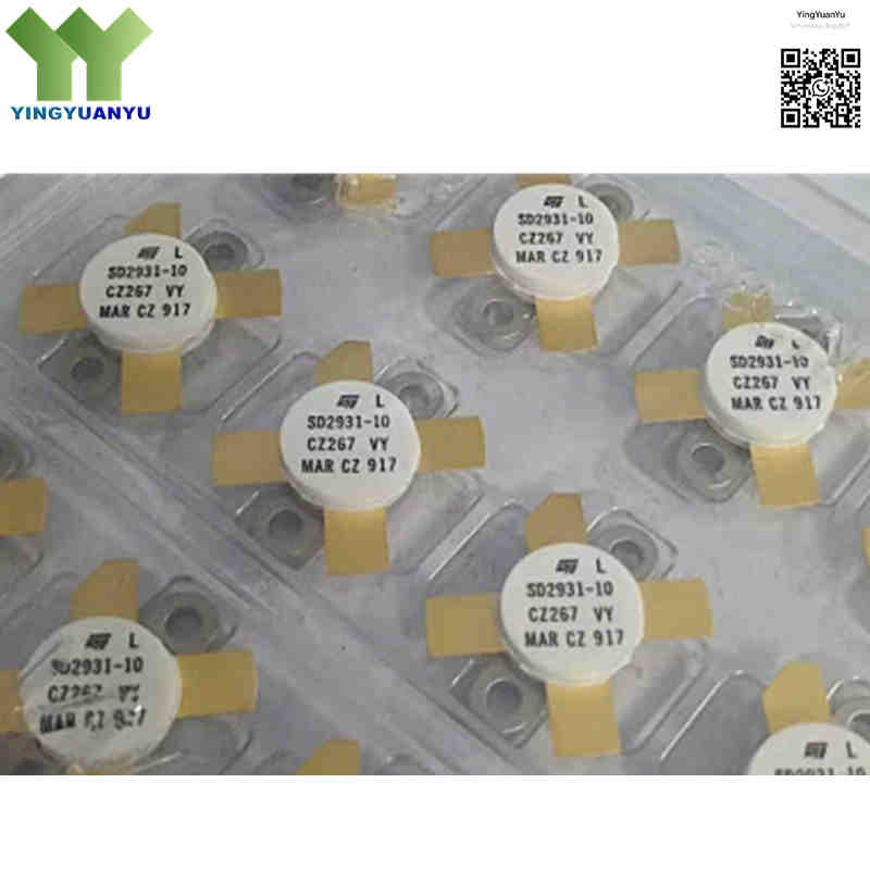
SD2931-10
| Part Number | SD2931-10 |
|---|---|
| Manufacturer | STMicroelectronics |
| Category | Discrete Semiconductor Products > Transistors – FETs, MOSFETs – RF |
| Description | N‑Channel RF Power MOSFET Transistor, 150W Output Power, 50V, 175 MHz operating frequency, M174 / Flanged Package. |
| Stock Status | In Stock |
| Origin | Original Factory |
Product Overview
The SD2931‑10 is gold‑metallized N‑channel RF DMOS power transistor for 50‑V HF/VHF amplifier applications up to 175 MHz. It delivers minimum 150 W output power, with 25% lower thermal resistance compared to standard SD2931 for improved continuous‑power reliability. Housed in M174 flanged ceramic package.
Core Advantages
High Output Power & Gain
150 W minimum output power @175 MHz, typical 14 dB gain, high PAE, reduces drive‑power demand.
Superior Load‑Mismatch Ruggedness
Withstands 20:1 VSWR without device damage, ensures stable operation under abnormal load conditions.
Gold‑Metallized DMOS Process
Enhanced electromigration resistance, longer service life and stable high‑frequency performance.
Optimized Thermal Characteristic
25% lower thermal resistance versus SD2931, suitable for long‑time continuous high‑power transmission.
M174 Flanged Ceramic Package
Low junction‑case thermal resistance (Rth(j‑c)=0.45℃/W), easy heat‑sink assembly for high‑power systems.
Key Specifications
| Brand | STMicroelectronics |
|---|---|
| RoHS Status | RoHS Compliant / Lead‑Free |
| EDA / CAD | PCB Footprint & 3D Model Available upon Request |
| Warranty | 1‑Year Standard Quality Warranty |
| Package / Case | M174 / M243 Flanged Ceramic Package |
| Mounting Type | Chassis Mount / Flange Mount |
| Surface Marking / Silkscreen | SD2931‑10 / ST Logo |
| Transistor Type | N‑Channel RF Power MOSFET (DMOS) |
| Drain‑Source Voltage (Vdss) | 125 V |
| Operating Drain Voltage (Vdd) | 50 V |
| Drain Current (Id) | 20 A |
| Power Dissipation(Pd) | 389 W (Tc=25℃) |
| Output Power (Pout) | 150 W min. |
| Frequency Range | HF to 175 MHz |
| Power Gain | > 15 dB (at 175 MHz, 50V) |
| Junction‑Case Thermal Resistance(Rth(j‑c)) | 0.45 ℃/W |
| Max Operating Junction Temperature(Absolute Maximum Rating) | 200°C (Absolute destructive limit, measured at Tcase=25°C) |
| Storage Temperature Range | -65°C ~ +150°C (Non‑operating) |
Typical Applications
- FM Broadcast Transmitters and High‑Power Radio Repeaters
- HF/VHF Tactical and Commercial Communication Amplifiers
- Industrial, Scientific, and Medical (ISM) RF Generators (CO2 Laser Drivers, Plasma Heating)
- Nuclear Magnetic Resonance (NMR) and Medical Resonance Imaging Equipment
- Avionics and Marine VHF Communications Systems
Order & Shipping Info
| Minimum Order Quantity (MOQ) | 1 Piece |
|---|---|
| Shipping Time | Shipped within 1‑2 business days |
| Delivery Time | 3‑7 working days worldwide |
| Shipping Methods | DHL, UPS, FedEx, EMS |
| Payment Methods | T/T (Bank Transfer), PayPal, Credit Card, Western Union |
Technical Support
For datasheet, sample requests, stock check, or bulk pricing, please use the Quick Inquiry form. We will reply within 24 hours.
Frequently Asked Questions
Q1: What is the main operating frequency and output power rating of SD2931‑10?
A: SD2931‑10 works up to 175 MHz, minimum 150 W output power at 50 V operating drain voltage.
Q2: How rugged is the SD2931‑10 against load mismatch?
A: It handles up to 20:1 VSWR across all phase angles at rated power without damage or performance degradation.
Q3: What package format is used for the SD2931‑10?
A: M174 (M243) flanged ceramic package, optimized for chassis mounting and low thermal resistance.
Q4: What is the difference between SD2931 and SD2931‑10?
A: Pin‑to‑pin compatible with identical electrical specs. SD2931‑10 has 25% lower thermal resistance for continuous high‑power operation.
Q5: What does suffix ‑W stand for in SD2931‑10W?
A:‑W means plastic tray loose packing. Chip and electrical parameters are exactly the same as SD2931‑10.
Q6: Are there pin‑to‑pin compatible replacement parts for SD2931‑10?
A: SD2931 is direct pin‑compatible alternative with higher thermal resistance. Other brand devices require re‑design of matching and bias circuits.
Q7: What are thermal limits for SD2931‑10?
A: Absolute maximum junction temperature 200°C (destructive limit, Tcase=25°C). Storage temperature:‑65°C ~ +150°C. Proper heat‑sink is mandatory for high‑power operation.
Q8: How can I request datasheets, CAD files or bulk quotations?
A: Submit Quick Inquiry form for datasheet, CAD footprint, stock check and volume pricing.
Related Products

