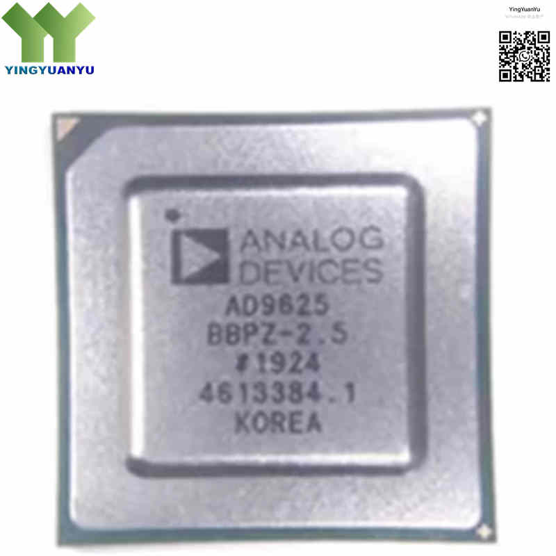
AD9625BBPZ-2.5
| Part Number | AD9625BBPZ-2.5 |
|---|---|
| Manufacturer | Analog Devices Inc. (ADI) |
| Category | Integrated Circuits (ICs) > Data Acquisition – Analog to Digital Converters (ADC) |
| Description | 12-Bit, 2.5 GSPS Monolithic Analog-to-Digital Converter (ADC) with integrated wideband input buffer and JESD204B high-speed serial data outputs. |
| Stock Status | In Stock |
| Origin | Original Factory |
Product Overview
The AD9625BBPZ-2.5 is a cutting-edge, 12-bit monolithic analog-to-digital converter (ADC) engineered by Analog Devices, designed to deliver exceptional conversion speeds up to 2.5 GSPS (Gigasamples per second). This ultra-high-speed device is optimized for capturing wideband signals across wide instantaneous bandwidths extending up to the second Nyquist zone. It incorporates an on-chip, wideband differential input buffer that stabilizes input impedance across high frequencies, simplifying the analog front-end (AFE) layout. To manage the immense data rate generated at 2.5 GSPS, the utilizes a high-speed JESD204B serial data interface configured for up to 8 lanes, significantly reducing digital track congestion on the host PCB. Outfitted with an advanced internal reference, digital downconverters (DDCs), and decimation filtering blocks, this high-performance ADC provides an exceptional dynamic range, making it a critical asset in radar processing, electronic warfare, wideband telecommunications, and advanced electronic test instrumentation pipelines.
Core Advantages
Ultra-Fast 2.5 GSPS Sampling Rate
Provides an industry-leading digitizing capability that allows designers to capture massive RF spectrum swaths directly, minimizing the complexity of multi-stage analog downconversion architectures.
Advanced JESD204B Serial Interface
Features an enterprise-grade 8-lane JESD204B serial output link operating up to 6.5 Gbps per lane, drastically reducing digital pin counts and layout constraints compared to traditional parallel LVDS architectures.
Integrated Wideband Input Buffer
Incorporates a highly linear internal differential buffer that ensures a uniform input impedance over the entire operating bandwidth, protecting signal integrity from sample-and-hold switching transients.
Flexible On-Chip Digital Processing
Houses native digital downconverters (DDCs) paired with configurable decimation filter blocks, allowing users to reduce output data rates and focus processing resources exclusively on the target bandwidth of interest.
Key Specifications
| Brand | Analog Devices Inc. (ADI) |
|---|---|
| RoHS Status | RoHS Compliant / Lead-Free Standard (Green Package) |
| EDA/CAD Model | 3D Model & PCB Footprint Available upon request |
| Warranty | 1-Year Standard Factory Warranty |
| Package / Case | BGA-196 (12×12 mm) |
| Mounting Type | Surface Mount Technology (SMD/SMT) |
| Surface Marking / Silkscreen | AD9625BBPZ-2.5 Marking |
| ADC Core Resolution | 12-Bit Architecture |
| Maximum Conversion Speed | 2.5 GSPS (Gigasamples per second) |
| Analog Input Bandwidth (-3dB) | Up to 3.2 GHz wideband sampling capability |
| Digital Interface Subsystem | JESD204B Subclass 1 Serial Output (Configurable 4, 6, or 8 lanes) |
| Dynamic Performance Metrics | SNR = 57.5 dBFS, SFDR = 77 dBc at 1 GHz Analog Input (-1 dBFS) |
| Integrated Features | On-chip DDC, 2x or 4x Decimation Filters, and Internal Voltage Reference |
| Total Power Consumption | Approximately 3.6 Watts at max sampling configuration |
| Operating Temperature Range | -40°C to +85°C (Extended Industrial Thermal Specifications) |
Typical Applications
- Advanced Radar Systems, Phased Array Systems, and Electronic Warfare (EW) Jammers
- High-Speed Digital Oscilloscopes, Spectrum Analyzers, and Automated Test Equipment (ATE)
- Wideband Communications Infrastructures, Satellite Modems, and Software-Defined Radio (SDR)
- Direct RF Sampling Backends and Multichannel Electronic Surveillance Networks
- Advanced Scientific Research Labs, High-Energy Physics, and Fast Laser Pulse Digitization
Order & Shipping Info
| Minimum Order Quantity (MOQ) | 1 Piece |
|---|---|
| Shipping Time | Shipped within 1-2 business days |
| Delivery Time | 3-7 working days worldwide |
| Shipping Methods | DHL, UPS, FedEx, EMS |
| Payment Methods | T/T (Bank Transfer), PayPal, Credit Card, Western Union |
Technical Support
For datasheet, sample requests, stock check, or bulk pricing, please use the Quick Inquiry form. We will reply within 24 hours.
Frequently Asked Questions
Q1: Is your stock inventory of the AD9625BBPZ-2.5 completely original and factory-new?
A: Yes, we guarantee that all AD9625BBPZ-2.5 ADCs in our stock are 100% brand-new, authentic factory-original components from Analog Devices, strictly stored and handled in accordance with international anti-static ESD shielding and moisture-controlled packaging guidelines.
Q2: What is indicated by the “-2.5” suffix in the AD9625 part designation?
A: The “-2.5” designation specifies the maximum rated sampling speed of the ADC core, certifying that this device is officially qualified to run at full speed grades up to 2.5 GSPS.
Q3: How does the JESD204B Subclass 1 standard support synchronous multi-chip arrays?
A: JESD204B Subclass 1 integrates a dedicated SYSREF signal lane. This high-precision physical input enables deterministic latency synchronization across multiple AD9625 devices, which is critical for phase-matched phased array radar layouts and multi-channel applications.
Q4: How can our technical team access layout optimization reference templates or clock distribution schematics for this part?
A: Please complete our Quick Inquiry web form on this page with details about your processing parameters. Our application support desk will process your inquiry and dispatch the available technical documentation package within 24 hours.
Related Products