
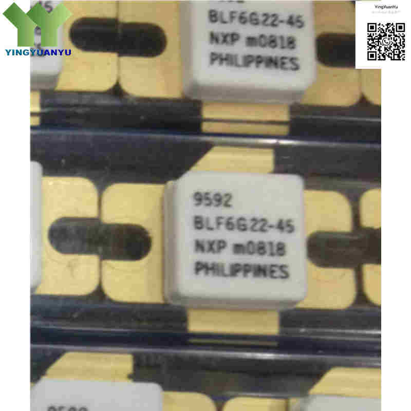
BLF6G22-45
| Part Number | BLF6G22-45 |
|---|---|
| Manufacturer | Ampleon / NXP Semiconductors |
| Category | Discrete Semiconductor Products / Transistors > RF FETs, MOSFETs |
| Description | 2.5W LDMOS Power Transistor, 2000 MHz to 2200 MHz Broadband Frequency Range, SOT608A Ceramic Flange Package. |
| Stock Status | In Stock |
| Origin | Original Factory |
Product Overview
BLF6G22‑45 is an N‑channel LDMOS RF power transistor from Ampleon (NXP), designed for 2000‑2200 MHz base‑station driver applications. It delivers typical 2.5 W CW output power at 28 V supply, with built‑in input matching and ESD protection. Housed in SOT608A ceramic flange package, it offers good linearity and ruggedness for W‑CDMA / LTE RF amplifier driver circuits.
Core Advantages
2.1GHz Band Driver Performance
Optimized for 2110‑2170 MHz cellular band, stable performance for multi‑carrier W‑CDMA and LTE driver stages.
High Gain & Efficiency
Typical 18.5 dB power gain with 13% drain efficiency, lowers thermal load for amplifier designs.
Built‑in Input Matching
Integrated input matching simplifies PCB layout and reduces external component count.
High Ruggedness
Withstands up to 10:1 VSWR mismatch; integrated ESD protection improves field reliability.
Key Specifications
| Brand | Ampleon / NXP Semiconductors |
|---|---|
| RoHS Status | RoHS Compliant / Lead-Free |
| EDA / CAD | PCB Footprint & 3D Model Available upon Request |
| Warranty | 1-Year Standard Quality Warranty |
| Package / Case | SOT608A / Flanged Ceramic Package |
| Mounting Type | Chassis Mount / Bolt-Down Flange Mount |
| Surface Marking / Silkscreen | BLF6G22-45 |
| Transistor Type | LDMOS (N-Channel Enhancement-Mode) |
| Operating Frequency Range | 2000 MHz to 2200 MHz (Broadband), typical 2110–2170 MHz |
| Output Power (Pout) | 2.5 W (Typical CW @28V) |
| Power Gain (Gps) | > 18.5 dB (Typical at 2140 MHz) |
| Drain Efficiency (ηD) | > 13% (Typical under 2-carrier W-CDMA) |
| Drain-Source Voltage (VDSS) | 65 V (Max Rating), 28V (Nominal Operating) |
| Gate-Source Voltage (VGS) | -0.5 V to +13 V (Operating Range) |
| Operating Junction Temperature (Tj) | Up to +225°C |
| Storage Temperature (Tstg) | -65 ℃ ~ +150 ℃ |
| Thermal Resistance (Rth(jc)) | 1.7 K/W (Junction to Case) |
| ACPR (Adjacent Channel Power Ratio) | < -49 dBc (Typical) |
Typical Applications
- 3G W-CDMA and 4G LTE Cellular Base Station Power Amplifier Driver Stages
- Macrocell and Microcell Wireless Communication Infrastructure
- Driver and Intermediate Stages in Doherty Power Amplifier Architectures
- Repeaters, Remote Radio Heads (RRH), and Distributed Antenna Systems (DAS)
- Industrial and Commercial 2.1 GHz Band Signal Amplifier Drivers
Order & Shipping Info
| Minimum Order Quantity (MOQ) | 1 Piece |
|---|---|
| Shipping Time | Shipped within 1-2 business days |
| Delivery Time | 3-7 working days worldwide |
| Shipping Methods | DHL, UPS, FedEx, EMS |
| Payment Methods | T/T (Bank Transfer), PayPal, Credit Card, Western Union |
Technical Support
For datasheet, sample requests, stock check, or bulk pricing, please use the Quick Inquiry form. We will reply within 24 hours.
Frequently Asked Questions
Q1: What frequency range does BLF6G22‑45 support?
A: Broadband 2000‑2200 MHz, optimized for 2110‑2170 MHz 2.1GHz W‑CDMA / LTE cellular band.
Q2: What is the output power of BLF6G22‑45?
A: Typical 2.5W CW @28V DC. Note: suffix “45” is not power rating, it is a driver‑stage LDMOS transistor.
Q3: How to handle thermal design for SOT608A package?
A: Bolt the ceramic flange firmly to smooth heatsink with thermal grease for low thermal resistance.
Q4: Difference between BLF6G22‑45,135 and BLF6G22‑45,112?
A: ,135 / ,112 are order suffixes for batch & packaging. Die, specs, pinout and package are identical, direct pin‑to‑pin replacement. Both are EOL, stock‑only components.
Q5: What is recommended replacement for BLF6G22‑45?
A: Ampleon official alternative: BLM7G1822S‑40PBG, better linearity for 2GHz base‑station driver application.
Q6: Can BLF6G22‑45 be used for final power amplifier stage?
A: No, it is designed for driver stage. Use higher‑power LDMOS like BLF6G22‑100 for final PA.
Q7: Does BLF6G22‑45 include internal input matching?
A: Yes, built‑in input matching reduces external components and simplifies PCB layout.
Q8: What is the VSWR ruggedness rating?
A: Survives 10:1 full‑phase load mismatch at 28V supply for high amplifier circuit robustness.
Related Products

