
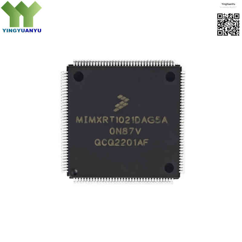
IMXRT1021DAG5A
| Part Number | IMXRT1021DAG5A |
|---|---|
| Manufacturer | NXP Semiconductors |
| Category | Integrated Circuits (ICs) > Embedded – Microcontrollers (i.MX RT1020 Crossover MCUs) |
| Description | i.MX RT1020 Crossover MCU, ARM Cortex-M7 Core, 500 MHz, 256KB SRAM, High-Speed Interfaces, 144-LQFP Package. |
| Stock Status | In Stock |
| Origin | Original Factory |
Product Overview
The MIMXRT1021DAG5A is a high-performance crossover MCU of NXP i.MX RT1020 series, built on ARM Cortex-M7 core up to 500MHz. Equipped with 256KB configurable on-chip SRAM, dual Ethernet, CAN-FD and USB 2.0 OTG peripherals, this 144-pin LQFP chip fits industrial controllers, smart grid, medical monitoring and consumer IoT devices.
Core Advantages
Extreme Performance ARM Cortex-M7 Core
500MHz operation with double-precision FPU, supporting motor control, high-speed data and DSP audio calculation.
Flexible Tightly Coupled Memory (TCM)
256KB RAM configurable as I-TCM/D-TCM, delivering single-cycle execution for critical program loops.
Rich Industrial Connectivity
Dual 10/100 Ethernet, CAN-FD and high-speed USB simplify industrial bus data transmission without extra controllers.
Cost-Effective Packaging
Standard 144-pin LQFP supports common 4-layer PCB designs, cutting assembly costs vs dense BGA packages.
Key Specifications
| Brand | NXP i.MX RT1020 Series |
|---|---|
| Full Part Number | MIMXRT1021DAG5A |
| RoHS Status | RoHS Compliant / Lead-Free |
| EDA/CAD Model | Schematic symbol, layout footprints, and IBIS simulation files are available on request |
| Warranty | 1-Year Standard Quality Warranty |
| Package / Case | 144-LQFP (20mm × 20mm) |
| Mounting Type | Surface Mount |
| Surface Marking / Silkscreen | MIMXRT1021DAG5A Marking |
| Core Architecture | ARM Cortex-M7 with 16KB I-Cache and 16KB D-Cache |
| Maximum Clock Speed | 500 MHz |
| On-Chip RAM | 256 KB (Configurable as Instruction/Data TCM or System RAM) |
| I/O Count | 96 General Purpose I/O Pins |
| ADC Resolution | 12-bit Multi-channel Analog-to-Digital Converter |
| External Memory Interface | SDRAM (up to 166 MHz clock), Parallel NOR/NAND Flash, and Quad/Octal SPI serial Flash |
| Network Connectivity | 2 × 10/100 Mbps Ethernet controllers (IEEE 1588 compliant) |
| Communication Interfaces | 1 × USB 2.0 High-Speed OTG with integrated PHY, 2 × CAN (including CAN-FD), 8 × LPUART, 4 × LPSPI, 4 × LPI2C |
| Operating Voltage (VDD) | 3.0V to 3.6V (peripherals) / Integrated DCDC converter for internal core supplies |
| Operating Temperature Range | -40°C to +85°C (Industrial-grade qualification) |
| FPU Support | Single & Double Precision Floating Point Unit Built-in |
| DAC Channels | 2-channel 12-bit Digital-to-Analog Converter |
| PWM Modules | Multiple FlexPWM Modules for Motor Control |
Typical Applications
- Industrial automation controllers, programmable logic controllers (PLCs), and variable frequency drives (VFD)
- Professional audio gear, multi-channel voice synthesis devices, and sound synthesis synthesizers
- Smart metering infrastructure, environmental monitoring systems, and local sensor gateways
- Low-latency building automation control hubs and smart lighting networks
- Hospitals and personal medical equipment requiring robust real-time graphical rendering and fast analysis
Order & Shipping Info
| Minimum Order Quantity (MOQ) | 1 Piece |
|---|---|
| Shipping Time | Shipped within 1-2 business days |
| Delivery Time | 3-7 working days worldwide |
| Shipping Methods | DHL, UPS, FedEx, EMS |
| Payment Methods | T/T (Bank Transfer), PayPal, Credit Card, Western Union |
Technical Support
For datasheet, sample requests, stock check, or bulk pricing, please use the Quick Inquiry form. We will reply within 24 hours.
Frequently Asked Questions
Q1: What is a crossover MCU like MIMXRT1021DAG5A?
A: It combines high-speed processor performance and rich peripherals with low-latency, easy-to-use MCU features. It has no built-in flash and runs programs from external high-speed memory.
Q2: Why TCM memory matters for this chip?
A: TCM is high-speed RAM directly connected to Cortex-M7 core. The 256KB RAM split into I-TCM and D-TCM enables single-cycle access at 500MHz, eliminating cache delay for real-time tasks.
Q3: Where does the chip store firmware without internal flash?
A: It boots from external QSPI / HyperFlash via FlexSPI controller. XIP technology lets it execute programs directly from cheap external flash with near on-chip flash speed.
Q4: Does MIMXRT1021DAG5A integrate power management?
A: Yes, it contains built-in DC-DC converter and LDO regulators. Only a single 3.3V external power supply is needed, simplifying PCB layout design.
Q5: Are free samples available for testing?
A: We support small free sample orders for prototype verification. Fill in the inquiry form to apply for samples and stock confirmation.
Q6: What is the lead time for bulk orders of this model?
A: Regular stock items ship within 1-2 working days. Out-of-stock bulk orders take 4-8 weeks based on factory production schedules.
Q7: Is this component industrial temperature grade?
A: Yes, its operating temperature range covers -40°C ~ +85°C, suitable for industrial control, medical and outdoor IoT equipment.
Q8: Can you provide official original datasheet?
A: Original NXP datasheet is attached upon inquiry submission, including electrical parameters, pinout diagram and PCB layout guides.
Related Products

