
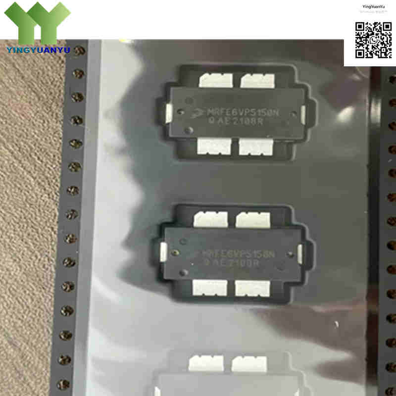
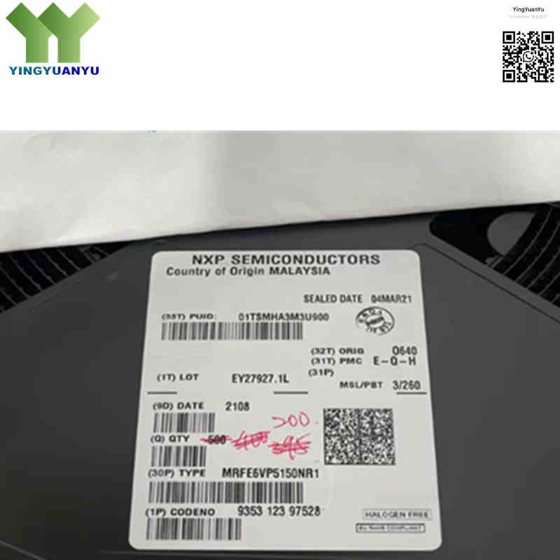
MRFE6VP5150NR1
| Part Number | MRFE6VP5150NR1 |
|---|---|
| Manufacturer | NXP Semiconductors / Freescale |
| Category | Discrete Semiconductor Products > Transistors – FETs, MOSFETs – RF |
| Description | High Ruggedness RF Power LDMOS Transistor, 150W CW, 1.8 to 600 MHz, 50V, TO‑270WB‑4 (OM‑780‑2) Package. |
| Stock Status | In Stock |
| Origin | Original Factory |
Product Overview
The MRFE6VP5150NR1 is a high‑ruggedness NXP LDMOS RF power transistor. It delivers 150 W CW output power at 50 V, covering 1.8‑600 MHz. Featuring >65:1 VSWR load‑mismatch tolerance and on‑chip ESD protection, it is ideal for high‑reliability RF power amplifier applications including broadcast, ISM and radar systems.
Core Advantages
Superior Load‑Mismatch Ruggedness
Withstands >65:1 VSWR across all phase angles without device damage, ensuring stable operation under harsh load conditions.
Wide Frequency & High Gain
Covers 1.8‑600 MHz with 26.3 dB typical gain at 230 MHz, reducing required driver stage count.
High‑Efficiency 50 V Operation
50 V DC operation enables high efficiency, lower operating current and simplified matching circuit design.
Robust Package & ESD Protection
TO‑270WB‑4 (SOT‑1736‑1 / OM‑780‑2) flange package with low thermal resistance and integrated on‑chip ESD protection.
Key Specifications
| Brand | NXP Semiconductors / Freescale |
|---|---|
| RoHS Status | RoHS Compliant / Lead‑Free |
| EDA / CAD | PCB Footprint & 3D Model Available upon Request |
| Warranty | 1‑Year Standard Quality Warranty |
| Package / Case | TO‑270WB‑4 (OM‑780‑2, Over‑molded Plastic Flanged) |
| Mounting Type | Chassis Mount / Flange Mount |
| Surface Marking / Silkscreen | MRFE6VP5150N Marking |
| Transistor Type | LDMOS N‑Channel RF Power MOSFET |
| Frequency Range | 1.8 MHz to 600 MHz |
| Output Power (Pout) | 150 W CW / 150 W Pulsed Peak (100μs, 20% duty cycle) |
| Operating Drain Voltage (Vdd) | 50 V DC Typ. (Max 133V Vdss Breakdown) |
| Power Gain (Gps) | 26.3 dB Typ. @ 230 MHz |
| Drain Efficiency | > 60% Typ. (Depending on frequency and bias) |
| Operating Junction Temperature | -40°C to +225°C |
| Load Mismatch Tolerance | >65:1 VSWR, all phase angles, no device degradation |
| ESD Protection | Integrated ESD protection on‑chip |
| Package Suffix Variants | NR1: Tape‑and‑Reel; GNR1: Bulk tray packaging |
Typical Applications
- VHF/UHF Analog and Digital TV Broadcasters and Radio Transmitters
- Industrial, Scientific, and Medical (ISM) RF Generators (Laser, Plasma, CO2)
- CO2 Laser Drivers and Ultrasonic Generators
- Avionics, Radar Systems, and Military Tactical Radios
- HF, VHF, and UHF Land Mobile Communications and Amateur Radio Amplifiers
Order & Shipping Info
| Minimum Order Quantity (MOQ) | 1 Piece |
|---|---|
| Shipping Time | Shipped within 1‑2 business days |
| Delivery Time | 3‑7 working days worldwide |
| Shipping Methods | DHL, UPS, FedEx, EMS |
| Payment Methods | T/T (Bank Transfer), PayPal, Credit Card, Western Union |
Technical Support
For datasheet, sample requests, stock check, or bulk pricing, please use the Quick Inquiry form. We will reply within 24 hours.
Frequently Asked Questions
Q1: What operating frequency range does MRFE6VP5150NR1 support?
A: The MRFE6VP5150NR1 supports a wide frequency range from 1.8 MHz to 600 MHz.
Q2: What is the power output and recommended drain supply voltage?
A: It delivers 150 W CW output power at 50 V DC drain supply. Peak pulsed power reaches 150 W under 100 μs, 20% duty‑cycle condition.
Q3: How robust is MRFE6VP5150NR1 under severe load mismatch?
A: It features excellent ruggedness, handling >65:1 VSWR across all phase angles without device failure or performance degradation.
Q4: What is the difference between MRFE6VP5150NR1 and MRFE6VP5150GNR1?
A: NR1 is tape‑and‑reel for SMT assembly; GNR1 is bulk tray packaging. Die, electrical performance and package outline are identical, only delivery form differs.
Q5: What is the package outline of MRFE6VP5150NR1?
A: It uses TO‑270WB‑4 flange plastic package. SOT‑1736‑1 / OM‑780‑2 are NXP internal codes. Designed for chassis‑mount heat‑sink installation.
Q6: Are there pin‑to‑pin compatible replacement parts?
A: MRFE6VP5150GNR1 is pin‑to‑pin compatible (only packaging difference). No other direct pin‑to‑pin replacement models are available. For higher‑power options, please contact us for custom selection. Always verify voltage, frequency and power rating before substitution.
Q7: Does MRFE6VP5150NR1 have built‑in ESD protection?
A: Yes, integrated on‑chip ESD protection is included. Still apply standard anti‑static handling during assembly and installation.
Q8: What precautions for assembly and handling?
A: Follow anti‑static handling rules. Ensure good thermal interface between flange and heat sink. Keep junction temperature below 225°C maximum rating.
Q9: How can I request datasheets, S‑parameter models or volume quotes?
A: Full technical documents, S‑parameter files and volume price quotes can be requested via our Quick Inquiry form.
Related Products

