
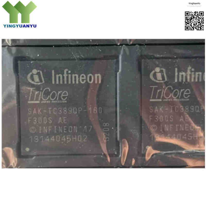
SAK-TC389QP-160F300S AE
SAK‑TC389QP‑160F300S AE
| Part Number | SAK-TC389QP-160F300S AE |
|---|---|
| Manufacturer | Infineon Technologies |
| Category | Integrated Circuits (ICs) > Embedded – Microcontrollers |
| Description | 32‑Bit AURIX™ TC38x Quad TriCore™ Microcontroller, 300MHz, 10MB ECC‑Protected Flash, PG‑LFBGA‑516 Package, ISO 26262 ASIL‑D. |
| Stock Status | In Stock |
| Origin | Original Factory |
Product Overview
The SAK‑TC389QP‑160F300S AE is Infineon’s high‑performance 32‑bit AURIX™ TC38x automotive microcontroller. It features four TriCore™ v1.6.2 cores (300 MHz), 2 lock‑step checker cores, 10 MB ECC‑protected Flash and 1.34‑1.53 MB ECC‑protected SRAM. Compliant with ISO 26262 ASIL‑D and IEC 61508 SIL‑3, it integrates a full‑feature eVita HSM, Gigabit Ethernet and abundant automotive peripherals, ideal for domain controllers and vehicle computing systems.
Note: The “160” in part number is memory/package variant identifier, not clock frequency. Actual CPU frequency is 300 MHz.
Core Advantages
Quad TriCore™ High‑Performance Processing
4×TriCore™ v1.6.2 cores up to 300 MHz with 2 lock‑step cores, delivering 2700 DMIPS with FPU/DSP for real‑time automotive control.
High‑Level Functional Safety (ASIL‑D)
Meets ISO 26262 ASIL‑D & IEC 61508 SIL‑3, with end‑to‑end memory ECC and hardware self‑diagnostics.
Advanced Hardware Security Module (HSM)
Full‑feature eVita‑High HSM supports hardware‑accelerated cryptography, ECC256/SHA2 and secure OTA firmware updates.
Rich Automotive Communication Interfaces
Equipped with Gigabit Ethernet, 12×CAN‑FD, 2×FlexRay, 24×LIN, 6×QSPI, 2×I2C, 25×SENT and 128×DMA for high‑speed vehicle networking.
Simplified Single‑Supply Power Design
Supports 3.3 V / 5 V single‑supply operation; on‑chip EVRC generates 1.25 V core voltage to simplify external power circuits.
ECC‑Protected Large Memory
10 MB ECC‑protected Flash (A/B mirror swap for safe OTA) and 1.34‑1.53 MB ECC‑protected SRAM for complex AUTOSAR applications.
Key Specifications
| Brand | Infineon Technologies |
|---|---|
| RoHS Status | RoHS Compliant / Lead‑Free |
| EDA / CAD | PCB Footprint & 3D Model Available upon Request |
| Warranty | 1‑Year Standard Quality Warranty |
| Package / Case | PG‑LFBGA‑516 (17×17 mm) |
| Mounting Type | Surface Mount (SMD / SMT) |
| Surface Marking / Silkscreen | SAK‑TC389QP‑160F300S AE,Marking |
| Core Architecture | Quad 32‑Bit TriCore™ v1.6.2, 2 hardware lock‑step checker cores, FPU+DSP, 2700 DMIPS |
| Clock Speed | Up to 300 MHz |
| Program Memory (Flash) | 10 MB ECC‑Protected Flash (supports A/B mirror swap) |
| SRAM Capacity | 1.34‑1.53 MB ECC‑Protected SRAM |
| Network Interfaces | Gigabit Ethernet, 12×CAN FD, 2×FlexRay, 24×LIN, 6×QSPI, 2×I2C, 25×SENT, 128×DMA, Multi‑Channel ADC/DAC/PWM |
| Safety Compliance | ISO 26262 ASIL‑D, IEC 61508 SIL‑3, integrated eVita HSM (ECC256 / SHA2) |
| Supply Voltage | Single‑supply 3.3 V / 5 V compatible; on‑chip EVRC generates 1.25 V core voltage |
| Operating Temperature | ‑40°C to +125°C (Ambient Ta); Max Junction Temperature Tj: 165°C |
Typical Applications
- Automotive Domain Controllers, Zone Controllers, and Central Vehicle Computers
- Advanced Driver Assistance Systems (ADAS) and Autonomous Driving fusion nodes
- Electric Vehicle (EV) Powertrain, Main Inverter, and High‑Voltage Management Systems
- Chassis Control, Electronic Power Steering (EPS), and Active Braking Control Units
- High‑end industrial automation controllers and multi‑axis motion robotics
Order & Shipping Info
| Minimum Order Quantity (MOQ) | 1 Piece |
|---|---|
| Shipping Time | Shipped within 1‑2 business days |
| Delivery Time | 3‑7 working days worldwide |
| Shipping Methods | DHL, UPS, FedEx, EMS |
| Payment Methods | T/T (Bank Transfer), PayPal, Credit Card, Western Union |
Technical Support
For datasheet, sample requests, stock check, or bulk pricing, please use the Quick Inquiry form. We will reply within 24 hours.
Frequently Asked Questions
Q1: How many CPU cores does SAK‑TC389QP‑160F300S AE have?
A: 4×TriCore™ v1.6.2 cores @300 MHz plus 2 hardware lock‑step checker cores, 2700 DMIPS with FPU/DSP support.
Q2: What is the flash & SRAM capacity?
A: 10 MB ECC‑protected Flash (supports A/B mirror swap for OTA); 1.34‑1.53 MB ECC‑protected SRAM.
Q3: What package is this part in?
A: PG‑LFBGA‑516, 516‑pin, 17×17 mm SMD. This package enables full peripherals including Gigabit Ethernet.
Q4: Where can I get datasheet & volume pricing?
A: Please submit inquiry form for datasheet, CAD files, real‑time stock and bulk quotation.
Q5: What do the part‑number suffixes mean?
A: SAK=automotive grade; QP=4‑core + full HSM; 160=memory/package variant(not frequency); 300=300 MHz; AE=silicon stepping revision.
Q6: Difference between TC389QP and TC387QP?
A: TC389QP has full‑feature HSM and complete peripheral set. TC387QP comes with reduced HSM and fewer interfaces for cost‑sensitive designs.
Q7: Are there pin‑compatible alternatives?
A: SAK‑TC389QP‑160F300S‑AA (earlier silicon stepping); SAK‑TC389QP‑96F300S‑AE (9.6 MB Flash). Firmware validation is required before substitution.
Q8: SAK vs SAL prefix for AURIX MCUs?
A: SAK = automotive‑grade with AEC‑Q100 qualification. SAL = industrial‑grade, same temperature range but no automotive certification.
Q9: Can all peripherals work at the same time?
A: No. Pins are multiplexed; some peripherals cannot be enabled simultaneously. Refer to official datasheet for pin‑mux configuration.
Q10: Difference between 516‑ball and 292‑pin packages?
A: PG‑LFBGA‑516 offers full peripherals (Gigabit Ethernet, max CAN‑FD/LIN). 292‑pin package has fewer I/O and limited functions for low‑end automotive applications.
Q11: What is the maximum junction temperature?
A: Ambient:‑40~+125°C; Max junction Tj:165°C. Follow datasheet thermal derating for real‑world designs.
Related Products

