
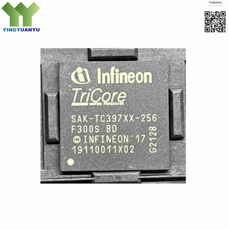
SAK-TC397XX-256F300S BD
SAK-TC397XX-256F300S BD
| Part Number | SAK-TC397XX-256F300S BD |
|---|---|
| Manufacturer | Infineon Technologies |
| Category | Integrated Circuits (ICs) > Embedded – Microcontrollers (MCU) |
| Description | AURIX™ TC3xx 32-bit Hexa-Core TriCore™ Microcontroller, 300 MHz, 16 MB ECC Flash, 2.528 MB ECC SRAM, ISO 26262 ASIL-D, LFBGA-292 Package, AEC-Q100 Automotive Grade. |
| Stock Status | In Stock |
| Origin | Original Factory |
Product Overview
The SAK‑TC397XX‑256F300S BD is Infineon second‑generation AURIX TC3xx automotive‑grade 32‑bit hexa‑core TriCore MCU running at 300 MHz. Four lockstep cores support ISO 26262 ASIL‑D safety. It integrates 16 MB ECC Flash with A/B‑Swap OTA, 2.528 MB ECC SRAM, EVITA‑Full HSM, Gigabit Ethernet, CAN‑FD and rich automotive peripherals. LFBGA‑292 package for domain controllers, ADAS and EV powertrain applications.
Core Advantages
Hexa‑Core TriCore 300 MHz
Six 32‑bit TriCore CPUs with four lockstep cores, delivering high real‑time performance for complex automotive algorithms and data processing.
ASIL‑D Functional Safety
Full‑memory ECC, MBIST and SMU safety unit, supports ISO 26262 ASIL‑D / IEC 61508 SIL‑3 for safety‑critical vehicle systems.
EVITA‑Full HSM Cybersecurity
Built‑in hardware security module provides secure boot, crypto acceleration and key management to defend against automotive network tampering and cyber‑attacks.
Rich Automotive Interfaces
Gigabit Ethernet, 12×CAN FD, FlexRay, LIN, QSPI, I²C, SENT and eMMC/SDIO, ideal for vehicle gateway and zone‑based electronic architectures.
Key Specifications
| Brand | Infineon Technologies |
|---|---|
| RoHS Status | RoHS Compliant, AEC-Q100 Grade 1 Qualified Automotive Grade |
| EDA / CAD | PCB Footprint & 3D Model Available upon Request |
| Warranty | 1-Year Standard Quality Warranty |
| Package / Case | LFBGA-292 (PG-LFBGA-292) |
| Mounting Type | Surface Mount Device (SMD/SMT) |
| Surface Marking / Silkscreen | SAK-TC397XX-256F300S BD |
| Core Processor | 32-bit TriCore™ Hexa-Core (6 Cores / 4 Lockstep Cores) |
| Maximum Speed | 300 MHz |
| Program Memory Size | 16 MB ECC Flash, supports A/B Swap OTA upgrade |
| RAM Size | 2.528 MB On-Chip ECC SRAM |
| Connectivity | Gigabit Ethernet, 12×CAN FD, 2×FlexRay, LIN, 6×QSPI, 2×I²C, 25×SENT, SPI, UART, HSSL, eMMC/SDIO |
| Security Features | EVITA Full Hardware Security Module (HSM), ECC full memory protection, lockstep core safety monitoring |
| Operating Supply Voltage | 2.97 V ~ 5.5 V single power supply, typical 3.3V / 5V, internal LDO generates core voltage |
| Operating Temperature | -40°C to +125°C (Automotive Grade 1, AEC-Q100) |
| Analog & Timing | ADC up to 76 input channels, 128-channel DMA, GTM, CCU6, GPT12 redundant timers |
| Functional Safety Level | ISO 26262 ASIL-D, IEC 61508 SIL-3 |
Typical Applications
- Automotive Domain and Zone Controllers (Central Vehicle Computers)
- Advanced Driver Assistance Systems (ADAS) and Autonomous Driving Gateways
- Electric Vehicle (EV) Powertrain Control Units (PCU), Inverters, and BMS
- Chassis Control, Active Suspension, and Electronic Power Steering (EPS)
- High-Speed Automotive Central Gateways and Telematics Control Units
Order & Shipping Info
| Minimum Order Quantity (MOQ) | 1 Piece |
|---|---|
| Shipping Time | Shipped within 1-2 business days |
| Delivery Time | 3-7 working days worldwide |
| Shipping Methods | DHL, UPS, FedEx, EMS |
| Payment Methods | T/T (Bank Transfer), PayPal, Credit Card, Western Union |
Technical Support
For datasheet, sample requests, stock check, or bulk pricing, please use the Quick Inquiry form. We will reply within 24 hours.
Frequently Asked Questions
Q1: What processor architecture does SAK‑TC397XX‑256F300S BD adopt?
A: It uses Infineon 32‑bit TriCore™ architecture, 6 cores @300 MHz, 4 cores operated in lockstep for functional safety.
Q2: What is its functional safety grade?
A: Complies with ISO 26262 ASIL‑D and IEC 61508 SIL‑3 for safety‑critical automotive systems.
Q3: What package is this MCU?
A: PG‑LFBGA‑292, 292‑ball LFBGA surface‑mount package.
Q4: How do I get datasheet, pinout or volume quotation?
A: Submit your request via quick inquiry form for datasheet, pin‑map, stock status and bulk price.
Q5: What is the difference between TC397XX, TC397XA and TC397XP?
A: Pin‑to‑pin compatible. TC397XX: general‑purpose, 2.528 MB SRAM; TC397XA: ADAS/radar, 6.9 MB SRAM; TC397XP: powertrain, 2.816 MB SRAM.
Q6: What does suffix BD stand for?
A: BD is the ordering suffix for LFBGA‑292 package, AEC‑Q100 Grade1 (-40℃~+125℃), general automotive domain‑control variant.
Q7: What are pin‑compatible alternative parts?
A: Direct pin‑compatible: TC397XA / TC397XP; cost‑down alternatives: TC375, TC387 series AURIX MCUs.
Q8: Does it support OTA firmware upgrade?
A: Yes, 16 MB Flash supports A/B‑Swap dual‑bank OTA, avoids bricking during firmware update.
Q9: Is memory equipped with ECC protection?
A: Flash and SRAM both support ECC error correction, enhancing reliability under harsh automotive temperature & vibration conditions.
Q10: Difference between SAK and SAF prefix?
A: SAK: standard AEC‑Q100 automotive grade for general ECU. SAF: higher screening grade for safety‑critical engine & chassis ECU.
Related Products

