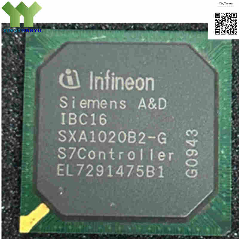
SXA1020B2-G
| Part Number | SXA1020B2-G |
|---|---|
| Manufacturer | Infineon Technologies |
| Category | RF/IF and RFID > RF Amplifiers |
| Description | High-linearity 10MHz to 2500MHz 1/4W broadband RF power amplifier. |
| Stock Status | In Stock |
| Origin | Original Factory |
Product Overview
The SXA1020B2-G is a highly linear, high-performance broadband RF power amplifier designed by Infineon Technologies. Operable across an incredibly broad frequency envelope from 10 MHz up to 2500 MHz, this versatile driver amplifier is explicitly optimized for infrastructure transmit chains that demand exceptional linearity, low noise floor interference, and robust power output configurations. It integrates a single-supply voltage operational matrix and internal active biasing circuitry that remains highly stable across fluctuating thermal spectrums. Housed in a compact, thermally-enhanced industry-standard surface-mount package, the serves as an ideal intermediate power stage or driver amplifier for cellular infrastructure base stations, wireless local loop systems, and multi-carrier broadband communication networks.
Core Advantages
Ultra-Wide Operational Frequency
Spanning seamlessly from 10 MHz up to 2.5 GHz, this device reduces components count and matching complexity by allowing a single amplifier layout to cover multiple wireless bands including VHF, UHF, cellular, and ISM channels.
Outstanding Linearity and ACPR
With excellent device characteristics, the device delivers an exceptional third-order intercept point (OIP3). This guarantees minimal intermodulation distortion and superb adjacent channel power ratio (ACPR) performance in multi-carrier architectures.
Integrated Active Internal Biasing
Features onboard active bias networks that automatically stabilize individual device currents against sudden shifts in operating temperature or voltage variations, eliminating external temperature-compensating peripheral networks.
Excellent Heat Dissipation & Robustness
The layout package features a dedicated exposed metallic backside pad that conducts operational thermal loads efficiently away from the chip, drastically extending the system’s Mean Time Between Failures (MTBF) under high-power environments.
Key Specifications
| Brand | Infineon Technologies |
|---|---|
| RoHS Status | RoHS Compliant / Lead-Free |
| EDA/CAD Model | 3D Model & PCB Footprint Available upon request |
| Warranty | 1-Year Standard Factory Warranty |
| Package / Case | BGA Package |
| Mounting Type | Surface Mount (SMD/SMT) |
| Surface Marking / Silkscreen | SXA1020B2-G Marking |
| Frequency Range | 10 MHz to 2500 MHz |
| Small Signal Gain | Typical 18 dB at 850 MHz (Application circuit dependent) |
| Output P1dB | +24 dBm (Typical 1/4 Watt RF Output) |
| Output IP3 (OIP3) | +40 dBm (Typical third-order intercept parameter) |
| Noise Figure | Typical 4.5 dB |
| Operating Voltage (V_cc) | Standard +5.0V Single Power Supply Rail |
| Operating Current | Typical 115 mA to 135 mA |
| Operating Temperature Range | -40°C to +85°C (Industrial Infrastructure Grade) |
Typical Applications
- Cellular Base Station Transmitters (W-CDMA, LTE, GSM, TD-SCDMA)
- Wireless Local Loop (WLL) and Wireless Broadband Access Backhauls
- Driver Stages for High-Power RF Base Station Power Amplifier Arrays
- Military Tactical Radios, UHF/VHF Communication Hubs, and ISM Equipment
- High-Dynamic-Range CATV Distribution Amplifiers and Cable Modems
Order & Shipping Info
| Minimum Order Quantity (MOQ) | 1 Piece |
|---|---|
| Shipping Time | Shipped within 1-2 business days |
| Delivery Time | 3-7 working days worldwide |
| Shipping Methods | DHL, UPS, FedEx, EMS |
| Payment Methods | T/T (Bank Transfer), PayPal, Credit Card, Western Union |
Technical Support
For datasheet, sample requests, stock check, or bulk pricing, please use the Quick Inquiry form. We will reply within 24 hours.
Frequently Asked Questions
Q1: Is your stock inventory of the SXA1020B2-G completely authentic and original?
A: Yes, we guarantee that all SXA1020B2-G RF amplifiers are 100% genuine, brand-new components from original factory production runs, complete with traceable batch and date codes.
Q2: What are the primary board layout considerations for matching the SXA1020B2-G across broad bands?
A: Due to its multi-octave bandwidth, optimizing broadband return loss values requires selecting appropriate external choke inductors and coupling capacitors. S-parameter simulation models are available upon request to assist with your layout.
Q3: Does the SXA1020B2-G require a negative voltage rail to bias the gate?
A: No, thanks to the advanced internal architecture, the chip includes its own internal active bias block and operates efficiently from a single standard +5V positive supply line.
Q4: How can we request specific application notes or evaluation boards for this part?
A: Please file a request via our Quick Inquiry web form on this page. Our technical RF applications group will respond with the requested PDF documentation and tooling options within 24 hours.
Related Products