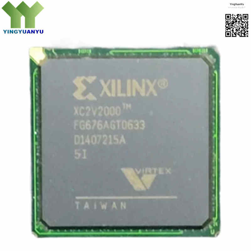
XC2V2000-5FG676I
| Part Number | XC2V2000-5FG676I |
|---|---|
| Manufacturer | Xilinx (AMD) |
| Category | Integrated Circuits (ICs) > Embedded – FPGAs (Field Programmable Gate Array) |
| Description | High-performance Virtex-II FPGA featuring 2 Million system gates, 26,880 logic cells, and 56 embedded multipliers, optimized for industrial-grade parallel computing and DSP acceleration. |
| Stock Status | In Stock |
| Origin | Original Factory |
Product Overview
The XC2V2000-5FG676I is a premier high-density, high-performance Field Programmable Gate Array (FPGA) built upon the field-proven Virtex-II® platform by Xilinx (now AMD). Specifically engineered to address compute-intensive digital signal processing (DSP), advanced networking protocols, and real-time embedded control, this device offers an impressive density of 2 million system gates and 26,880 core logic cells. Operating on a 1.5V core voltage using an 8-layer copper process, it seamlessly integrates advanced hardware resources including 56 dedicated 18×18-bit multipliers and a comprehensive SelectRAM™ memory hierarchy. Housed in a robust 676-pin fine-pitch ball grid array (FBGA) package, the delivers reliable, highly deterministic performance across extreme industrial operating temperature bands, making it a critical choice for aerospace telemetry, industrial automated machinery, data communications, and high-reliability instrumentation backplanes.
Core Advantages
Massive Parallel Computational Power
Equipped with 2 Million system gates and 56 dedicated hardware 18×18-bit multipliers, enabling rapid, multi-channel parallel processing of complex math algorithms like FFTs and digital filtering without degrading core logic routing.
Flexible SelectRAM™ Memory Hierarchy
Integrates a massive distribution of both internal Block RAM (1,008 Kbits) and highly configurable Distributed RAM resources, ensuring ultra-fast local data queuing and low-latency cache management directly adjacent to the execution logic.
Highly Adaptable SelectIO™ Ultra Hardware
Supports a massive selection of up to 19 single-ended and differential signaling standards (including high-speed LVDS, Bus LVDS, and PCI-X) alongside built-in Digitally Controlled Impedance (DCI) to guarantee flawless signal integrity over dense board layouts.
Industrial-Grade Thermal and Physical Longevity
Fully certified for continuous operation across the demanding industrial junction temperature range (-40°C to +100°C), providing exceptional electrical reliability and timing stability inside harsh industrial and military enclosures.
Key Specifications
| Brand | Xilinx (AMD) |
|---|---|
| RoHS Status | Non-RoHS Leaded Lead-Frame Construction (Optimized for aerospace, military, and critical industrial exemptions) |
| EDA/CAD Model | 3D Model & PCB Footprint Available upon request |
| Warranty | 1-Year Standard Factory Warranty |
| Package / Case | FBGA-676 (27x27mm) |
| Mounting Type | Surface Mount Technology (SMD/SMT) |
| Surface Marking / Silkscreen | XC2V2000™ Marking |
| FPGA Family Subsystem | Virtex-II® Platform Architecture |
| Total System Gates | 2,000,000 Gates |
| Logic Cells (LCs) Count | 26,880 Logic Cells |
| Total Embedded Block RAM | 1,008 Kbits (56 blocks x 18 Kbits each) |
| Dedicated 18×18 Multipliers | 56 Hardware Blocks |
| Maximum Available User I/O Pins | 456 Digital Input/Output Lines |
| Internal Core Operating Voltage | 1.425V to 1.575V DC (1.5V Nominal) |
| Operating Junction Temperature | -40°C to +100°C (Extended Industrial Grade Operational Profile) |
Typical Applications
- High-Speed Digital Signal Processing (DSP) & Real-Time Video/Image Processing Pipelines
- Aerospace Avionics, Military Radar Control Systems, and Telemetry Data Processing
- Industrial Robotics, Multi-Axis Motion Controllers, and Complex Automation Backplanes
- Telecommunication Infrastructure Networks, Basestations, and High-Throughput Protocol Bridges
- Advanced Test & Measurement Instrumentation, Data Acquisition Systems, and Medical Imaging Engines
Order & Shipping Info
| Minimum Order Quantity (MOQ) | 1 Piece |
|---|---|
| Shipping Time | Shipped within 1-2 business days |
| Delivery Time | 3-7 working days worldwide |
| Shipping Methods | DHL, UPS, FedEx, EMS |
| Payment Methods | T/T (Bank Transfer), PayPal, Credit Card, Western Union |
Technical Support
For datasheet, sample requests, stock check, or bulk pricing, please use the Quick Inquiry form. We will reply within 24 hours.
Frequently Asked Questions
Q1: Is your current stock inventory of the XC2V2000-5FG676I completely genuine and original?
A: Yes, we guarantee that all XC2V2000-5FG676I FPGAs in our warehouse are 100% brand-new, authentic factory-original products from Xilinx (AMD), managed and shipped strictly under compliant anti-static ESD shielding and moisture-controlled conditions.
Q2: What is decoded by the “-5FG676I” suffix sequence on this part number?
A: The “-5” designates the device’s high-speed performance grade tier. “FG676” refers directly to the 676-pin fine-pitch ball grid array package layout, and the terminal letter “I” indicates it is officially qualified to handle the Industrial thermal window (-40°C to +100°C).
Q3: Does this specific FG676 version contain lead (Pb) in its ball layout composition?
A: Yes, the “FG676” package variant uses traditional Sn/Pb (tin/lead) solder spheres. This is standard configuration and highly requested for high-reliability aerospace, defense, and long-lifecycle industrial systems where RoHS-exempt leaded connectivity is preferred to avoid tin-whisker risks.
Q4: How can our design engineers access legacy bitstream development support or older ISE design suite guidelines for this FPGA?
A: Please complete our Quick Inquiry web form on this page with details about your processing parameters. Our application support desk will process your inquiry and dispatch the available technical documentation package within 24 hours.
Related Products