XC7K160T-2FFG676I
| Part Number | XC7K160T-2FFG676I |
|---|---|
| Manufacturer | Xilinx (AMD) |
| Category | Integrated Circuits (ICs) > Embedded – FPGAs (Field Programmable Gate Array) |
| Description | Kintex-7 Field Programmable Gate Array, 162240 Logic Cells, 600 DSP Slices, 11700 Kb BRAM, 12.5 Gbps GTX Transceivers, Industrial Grade, FFG-676 (27.0 × 27.0 × 1.0mm) package. |
| Stock Status | In Stock |
| Origin | Original Factory |
Product Overview
The XC7K160T-2FFG676I is a high-performance, mid-range Field Programmable Gate Array (FPGA) from Xilinx (AMD), part of the advanced Kintex®-7 family. Built on a 28nm HKMG (High-K Metal Gate) process, it delivers exceptional logic density, ultra-fast signal processing, and optimized power efficiency. With 162,240 logic cells, 600 dedicated DSP48E1 slices, and 11,700 Kb of internal BRAM, it easily handles complex mathematical operations, parallel computing, and dense logic routing. It also integrates 8 high-speed GTX transceivers operating up to 12.5 Gbps, supporting bandwidth-heavy protocols like PCIe Gen2, Gigabit Ethernet, and CPRI. Packaged in a compact FFG-676 (27.0 × 27.0 × 1.0mm) BGA and qualified for industrial temperatures (-40°C to +100°C), this FPGA is ideal for high-throughput networking, military communications, electronic warfare, high-resolution medical imaging, and multi-axis industrial motion control.
Core Advantages
- Optimal Cost-to-Performance Ratio: Offers high-density logic cells, high-capacity DSP slices, and ultra-fast transceivers typically reserved for premium FPGAs, while maintaining the price and power profile of mid-range electronics.
- Exceptional Parallel DSP Processing: Features 600 dedicated hardware DSP48E1 slices that execute asymmetric math operations at top-tier speeds, enabling flawless multi-channel digital filtering, radar analytics, and real-time audio/video processing.
- High-Speed 12.5 Gbps Transceivers: Houses 8 integrated low-jitter GTX transceivers capable of running up to 12.5 Gbps per lane, facilitating native implementations of PCI Express Gen2 x8, Gigabit Ethernet, CPRI, and SATA standards.
- Rugged Industrial Longevity: Built to operate continuously across the extended industrial junction temperature span (-40°C to +100°C), guaranteeing unwavering timing accuracy and architectural reliability in severe environments.
Key Specifications
| Brand | Xilinx (AMD) |
|---|---|
| RoHS Status | RoHS Compliant / Lead-Free Standard (Green Packaging) |
| EDA/CAD Model | 3D Model & PCB Footprint Available upon request |
| Warranty | 1-Year Standard Factory Warranty |
| Package / Case | FFG-676 (27.0 × 27.0 × 1.0mm) |
| Mounting Type | Surface Mount Technology (SMD/SMT) |
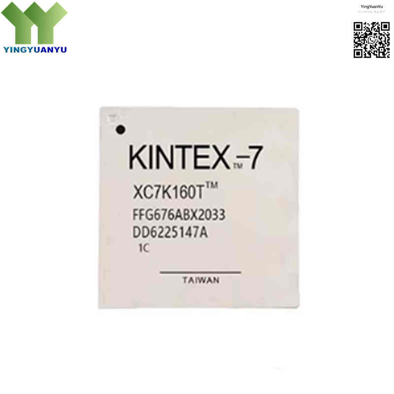
| Surface Marking / Silkscreen | XC7K160T™ / FFG676 Marking |
| FPGA Family Architecture | Kintex®-7 Platform Subsystem |
| Total Logic Cells Count | 162,240 Logic Cells |
| Total Programmable Logic Blocks (CLBs) | 25,350 Slices |
| Total Embedded Block RAM (BRAM) | 11,700 Kb (325 Blocks of 36 Kbits each) |
| Dedicated Hardware DSP Slices | 600 Multi-Function DSP48E1 Blocks |
| High-Speed Serial Transceivers | 8 GTX Transceivers (Operating up to 12.5 Gbps per lane) |
| Maximum Digital User I/O Lines | 400 Single-Ended I/Os (Supporting both high-performance and high-range signaling) |
| Operating Junction Temperature | -40°C to +100°C (Industrial Grade Thermal Qualification) |
Typical Applications
- High-Speed Telecommunications Infrastructure, 4G/5G Wireless Basestations, and LTE Backhaul Bridges
- Military Electronics, Radar System Digital Backplanes, Software-Defined Radio (SDR), and Avionics Telemetry
- High-End Medical Diagnostic Imaging Modules (High-Resolution Ultrasound, MRI Data Capture, and CT Scanning)
- Industrial Machine Vision Pipelines, High-Speed Edge Video Processing, and Distributed Automated Controllers
- Advanced Test & Measurement Instruments, Logic Protocol Analysers, and Oscilloscope Data Processing Hubs
Order & Shipping Info
- Minimum Order Quantity (MOQ): 1 Piece
- Shipping Time: Shipped within 1-2 business days
- Delivery Time: 3-7 working days worldwide
- Shipping Methods: DHL, UPS, FedEx, EMS
- Payment Methods: T/T (Bank Transfer), PayPal, Credit Card, Western Union
Technical Support
For datasheet, sample requests, stock check, or bulk pricing, please use the Quick Inquiry form. We will reply within 24 hours.
Frequently Asked Questions
Q1: Is your current stock inventory of the XC7K160T-2FFG676I completely genuine and original?
A: Yes, we guarantee that all XC7K160T-2FFG676I FPGAs in our inventory are 100% brand-new, authentic factory-original products from Xilinx (AMD), strictly stored and shipped under anti-static ESD shielding and dry moisture-barrier packaging.
Q2: What is decoded by the characters in the product suffix “-2FFG676I”?
A: The “-2” designates the mid-high performance speed grade tier of the inner logic fabric. “FFG676” refers to the physical 676-ball Pb-free flip-chip BGA package (1.0 mm pitch), and the trailing letter “I” certifies that the device is qualified for Industrial operating junction temperature limits (-40°C to +100°C).
Q3: Does this chip require specialized development software, and is a licensing key mandatory?
A: The XC7K160T is fully supported by the Xilinx Vivado® Design Suite. Depending on the version deployed, a Vivado design edition license may be required to synthesize, route, and compile bitstreams for this specific density level.
Q4: How can our engineering group request specific hardware design reference files, pinout constraints, or bulk pricing discounts?
A: Please complete our Quick Inquiry web form on this page with details about your processing parameters. Our application support desk will process your inquiry and dispatch the available technical documentation package within 24 hours.
Related Products