
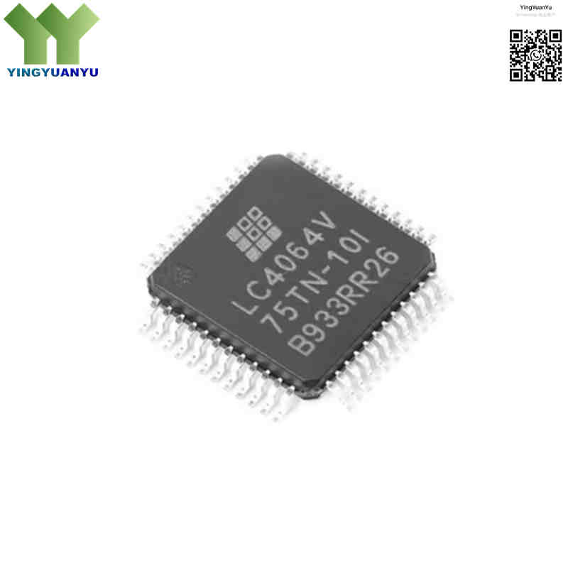
LC4064V-75TN48C
| Part Number | LC4064V-75TN48C |
|---|---|
| Manufacturer | Lattice Semiconductor |
| Category | Integrated Circuits (ICs) > Embedded – CPLDs (Complex Programmable Logic Devices) |
| Description | High-performance, low-power 3.3V SuperFAST ISP™ CPLD featuring 64 macrocells, 7.5ns propagation delay, and 32 user I/Os, housed in a lead-free 48-pin TQFP package. |
| Stock Status | In Stock |
| Origin | Original Factory |
Product Overview
LC4064V-75TN48C is a low-power 3.3V CPLD from Lattice ispMACH®4000V series. Equipped with 64 macrocells, 7.5ns signal delay and 32 user I/Os, it supports JTAG in-system programming without desoldering. Housed in lead-free 48-TQFP packaging, it is ideal for embedded logic control circuits.
Core Advantages
Ultra-Fast Timing Performance
7.5ns maximum pin-to-pin delay with symmetric routing, stable timing for high-speed logic design.
In-System Programmable (ISP™)
JTAG online programming supported; internal flash retains configuration, easy firmware upgrades without rework.
Low Power Design
Optimized circuit layout reduces static & dynamic power consumption, fit for compact, heat-sensitive devices.
Multi-Voltage I/O Compatibility
Independent I/O banks support 1.8V/2.5V/3.3V signals, serves as voltage conversion bridge for different ICs.
Key Specifications
| Brand | Lattice Semiconductor ispMACH® 4000V CPLD Product Family |
|---|---|
| RoHS Status | RoHS Compliant / Lead-Free / Green Halogen-Free Materials Sourced (“N” Suffix) |
| EDA/CAD Model | 3D STEP Models, Schematic Symbols, and Pinout Footprint Configurations available upon request |
| Warranty | 1-Year Standard Quality Warranty |
| Package / Case | 48-TQFP (7mm × 7mm × 0.50mm) |
| Mounting Type | Surface Mount Technology (SMD/SMT Lead-Free Reflow Solder Line Compatibility) |
| Surface Marking / Silkscreen | LC4064V Marking |
| Speed Grade | -75 (7.5ns maximum propagation delay) |
| Number of Macrocells | 64 Macrocells (organized in 4 GLBs / Generic Logic Blocks) |
| Propagation Delay | 7.5 ns maximum pin-to-pin signal transition speed |
| Maximum Clock Frequency | 168 MHz operational execution boundary |
| Number of Programmable I/Os | 32 User I/O lines available for custom routing configuration |
| Programming Interface Format | Standard IEEE 1149.1 4-wire JTAG Boundary Scan interface boundary |
| Core Operating Supply Voltage | 3.0 V to 3.6 V (Nominal 3.3 V single-rail operation framework) |
| Input/Output Voltage Interfacing | Supports multi-bank configuration down to 1.8V, 2.5V, and up to 3.3V logic signaling |
| Typical Operating Supply Current | 12mA @ 3.3V Static Current |
| Input Pin Capacitance | 8pF typical per I/O pin |
| Operating Temperature Range | 0°C to +90°C Commercial Operational Thermal Spectrum (T_J) |
| Storage Temperature Range | -55°C ~ +125°C |
Typical Applications
- High-Speed Microprocessor System Glue Logic, State Machine Maps, and Address Decoders
- Voltage Level Translation Bridges, I/O Expansion Multiplexers, and Power Sequencing Logic Controllers
- Industrial Control Instrumentation, Factory Automation Backplanes, and Communication Interface Modules
- Enterprise Telecom Routers, Edge Gateways, Data Storage Arrays, and Networking Hubs
- Embedded Single-Board Computers (SBC), Prototyping Evaluation Kits, and Medical Diagnostics Displays
Order & Shipping Info
| Minimum Order Quantity (MOQ) | 1 Piece |
|---|---|
| Shipping Time | Shipped within 1-2 business days |
| Delivery Time | 3-7 working days worldwide |
| Shipping Methods | DHL, UPS, FedEx, EMS |
| Payment Methods | T/T (Bank Transfer), PayPal, Credit Card, Western Union |
Technical Support
Request datasheets, samples, stock checking or bulk quotations via our inquiry form. We respond within 24 hours.
Frequently Asked Questions
Q1: Are LC4064V-75TN48C chips 100% original?
A: All CPLDs are brand new genuine Lattice original parts. We inspect batch codes and packages under ESD protection, shipped in anti-static trays to avoid pin damage.
Q2: What is the difference between LC4064V-75T48C and TN48C?
A: The “N” suffix stands for lead-free RoHS green packaging. Two versions are fully pin-to-pin and function compatible for SMT production.
Q3: Can the I/O pins connect to 1.8V microcontrollers?
A: Yes. I/O banks support separate Vcco power supply. Feed 1.8V to corresponding bank pins to realize 1.8V logic voltage conversion.
Q4: How to re-program the chip after soldering on PCB?
A: It supports 4-wire JTAG IEEE 1149.1 interface. Connect Lattice Diamond download cable to board JTAG pins to rewrite logic firmware.
Q5: Can I get free samples for testing?
A: Small test samples are available. Leave your required quantity and company info in the inquiry form for sample quotation.
Q6: What is the MOQ and delivery time?
A: MOQ is 1 piece for spot stock. Orders will be shipped within 1-2 working days, global delivery takes 3-7 days.
Q7: What is the quality warranty period?
A: We provide a 1-year quality warranty for all original parts. Contact us if you receive defective goods.
Q8: Do you support BOM full list matching and bulk discount?
A: We support one-stop BOM component matching. Better unit prices for large bulk orders, send your BOM for exclusive quotation.
Related Products

